
 Ultra High-Purity to Meet Your Needs
We produce the broadest range of Ultra High-Purity (UHP) chemistries focusing on the Electronics Industry. We’ve established a wide base of application specific products for the semiconductor industry.
Straight Acids and Bases
These are the backbone of wet processes. As device geometries continue to shrink and efforts to reduce defect densities grow, so has the demand for ultra high-purity chemicals. With over 30 years of experience in the production and purification of these chemistries, we offer a suite of finished products with down to 10 part-per-trillion (ppt) impurities.
Etchant Blends
Etchant blends selectively and uniformly remove substrates without damaging underlying layers, critical to wafer manufacturing. Our Etchant Blending expertise ranges from mainstream etchants to the development and manufacture of unique blends for customer-specific applications. These blends benefit from the high-purity levels of our base products.
Solvents
Soolvents and solvent blends are used extensively throughout the semiconductor industry for cleaning equipment, drying wafers and substrate deposition or removal. We have a large portfolio of high-purity solvents to address the needs of the electronics market.
Cleaning chemistries
Cleaning chemistries are critical for reducing defect densities and improving yields. Our innovations in cleaning mixtures have created new blends that reduce cost of ownership, are more environmentally friendly and focus on new interconnect/dielectric materials. Whether repairing the wafer surface for a thermal process, deposition of a substrate or removal of residues from the preceding operation, HEC offers the reliability that your manufacturing process requires. Proprietary blends are available.
 ULSI
Relates to SEMI Grade 2
Recommended for 0.80 – 1.20 µm technologies Trace Metals < 10 ppb
ULSI
Relates to SEMI Grade 2
Recommended for 0.80 – 1.20 µm technologies Trace Metals < 10 ppb
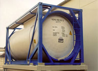
Supply Chain
We efficiently deliver the ultra high-purity product you need, where you need it and when you need it. Honeywell Electronic Chemicals combines patented packaging technology with our ability to optimize your shipping costs and maintain purity from the point of manufacture to consumption. Our chemical containers and dispensing systems maintain the highest product purity while maximizing safety and convenience.
Honeywell Electronic Materials has developed a patented, lower-cost, key coded, quick connect coupling system.
We’ve also designed new recyclable, low-cost polyethylene COEX drums and IBCs/totes, suitable for containing high-purity products either on a one-way or shuttle basis.
Quick Connect Coupling
Quick Connect Coupling is compatible with industry standard packaging. It protects personnel handling chemicals and it maintains the purity and quality of your shipments during closed production cycles.
Features of the Honeywell Quick Connect System:
• All components are plastic material.
• Gaskets made of universally chemical resistant perfluoroelastomers.
• Dispense head can be blocked with a check valve.
• You can code for the corresponding chemical.
• Standardized fittings for container threads.
• Meets or exceeds handling standards of high-purity electronic chemicals
Manufactured using injection molding process keeps your costs low
Conductive electric version available for specialty applications.
Safety & Environmental
Safe handling and transportation of HEM products are critical to your operation. With decades of experience, strict policies and guidelines enable us to manufacture, package our products safely to you. And we help you to ensure the same in your facilities.
We meet or exceed all local and federal safety and environmental guidelines. Our facilities minimize waste disposal and we’re continually looking for ways to improve our methods. We also run a container management and recycling process to maximize container life.
Precision Analysis Backs Up Our Product Integrity
Honeywell Electronic Chemicals maintains state-of-the-art analytical capabilities within our manufacturing facilities. We also develop our own proprietary methodologies to conduct analyses with extremely sensitive detection limits (down to 5 ppt levels).
Basic conditions and capabilities are the backbone of wet processes. As device geometries continue to shrink and efforts to reduce defect densities grow, so has the demand for ultra high-purity chemicals. With over 30 years of experience in the production and purification of these chemistries, we offer a suite of finished products with down to 10 part-per-trillion (ppt) impurities.
• On-site laboratories are certified to class 10, 000
• Samples are handled and prepared in class 100 and class 10 environments
• Detection levels for a variety of high-purity chemicals range from 1 ppb to 5 ppt depending on sample preparation and analysis techniques
• Detection levels for a variety of high-purity chemicals range from 1 ppb to 5 ppt depending on sample preparation and analysis techniques
• Gauge studies, correlation studies, and verified spike recoveries all traceable to NIST standards assure optimum accuracy
RELATED VIDEO


RELATED FACTS
- Dr. Patrick N. Keating is a theoretical physicist who has contributed to several fields of solid-state physics, including semiconductors, semi-insulators and the basic properties of solid materials, and to other fields including optics, liquid crystals, acoustic...
- Jennic Limited was a privately held UK-based fabless semiconductor company founded in 1996. The company developed a range of wireless microcontrollers that support low-power wireless standards, particularly 802.15.4, 6LoWPAN and ZigBee, and also supplied wireline...
-
 Magnetoresistance is the property of a material to change the value of its electrical resistance when an external magnetic field is applied to it. The effect was first discovered by William Thomson (more commonly known as Lord Kelvin) in 1856, but he was unable to...
Share this Post
latest post
-
 Semiconductor Processing November 26, 2023
 -
 Top Fabless Semiconductor companies October 27, 2023
 -
 Silicon Valley Semiconductor companies September 27, 2023
 -
 New Semiconductor companies August 28, 2023
 -
 List of Semiconductor companies in USA July 29, 2023
 -
 Semiconductor properties June 29, 2023
 -
 Semiconductor industry companies May 30, 2023
 -
 Canadian Semiconductor company April 30, 2023
 -
 Semiconductor companies in Europe March 31, 2023
 -
 Semiconductor jobs in Europe March 1, 2023
 -
 Freescale Semiconductor, Ltd January 30, 2023
 -
 Freescale Semiconductor Patent December 31, 2022
 -
 Freescale Semiconductor news December 1, 2022
 -
 Freescale Semiconductor stock symbol November 1, 2022
 -
 Global Semiconductor company October 28, 2022