

Wafers to be processed
Thin films of compound semiconductors are deposited or epitaxially grown on a substrate made of semiconductor materials or insulator like GaAs, InP, GaP, Sapphire, or SiC, and optical and functional devices are created on these substrates.
The substrate thickness is 0.25-1.0mm with a diameter of 2 to 5 inches (50 to 100mm), and the film is usually grown to a thickness of about 0.05-0.2mm. The substrate shape is usually round and so is called a wafer.
Front-end, back-end, and inspection processes
Once the wafers are prepared, a multi-step sequence is carried out to create the desired semiconductor devices. In general, optical semiconductor fabrication is grouped into two processes: the front-end process and the back-end process. In the front-end process, wafers are engineered, and in the back-end process, they are separated into individual elements or chips, and finally all the qualified chips are assembled into packages.
In the testing process to monitor each stage of serial processes, sampling or total inspection is conducted in accordance with procedures to administrate and control the processes and quality for a ultimate guarantee of quality.
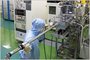
 Front-end process
The front-end process refers to the formation of the light-emitting and photo-detecting elements directly on the silicon or compound semiconductor wafer and provides a process flow in the procedure below.
Design of element function and related pattern
Design the functions and structures of some elements, according to customer demands.
Design and fabrication of photo-masks
Design and fabricate a photo-mask to transfer thousands of patterns of some element onto a glass plate.
Pattern formation
Create thousands of elements on a wafer. through the processes below.
- Film deposition (Process to grow a insulating film, such as oxide or nitride, onto the wafer.)
- Photolithography (Processes composed of coating photo-resist onto a whole wafer, transferring a pattern from a photo mask, exposure, development, and so on.)
- Etching (Chemical or physical microfabrication process to selectively remove parts of a insulating thin film or the bulk of a semiconductor material after UV light illumination onto the photo resist -coated wafer.)
- Impurity diffusion (Process to diffuse some dopant of p or n type into the very high-purity semiconductor wafers and modify electrical properties, forming P/N junction on the surface.)
The abovementioned steps are repeated to fabricate elements according to the process flow chart.
 Electrode formation
Make ohmic contacts with the p or n region, and, in an optical semiconductor element having polarity, the anode is the positive (+) electrode and the cathode is the negative (-) electrode.
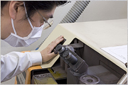
Wafer Inspection
Electrical performance is proved on a test machine, so-called a prover. This process is also known as wafer proving or wafer sorting test. All of individual elements connected on a wafer are subjected to such an electrical test for functional imperfections and are determined as good with meeting the requested specifications.
(1)Photomask alignment
(2)Thin film deposition
(3)Impurity diffusion
Back-end process
The back-end process consists of 4 steps: wafer mounting, die bonding, wire bonding, and packaging.
Wafer mounting
Mount a whole wafer onto an adhesive tape and attach it onto a ring before breaking it into individual pieces.
Wafer dicing
Cut a wafer containing thousands of elements into individual pieces, each called a die.
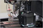
Die bonding
Mount or fix a die into the package or some substrate; also called die attachment.
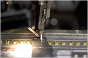
Wire bonding
Make interconnections between a die and the exterior of the package or substrate. The wire is attached at both sides by using some combination of heat, pressure, and ultrasonic energy to weld each end.
Visual inspection
Check visually die location, epoxy paste, and wiring.
Packaging
Encapsulate a die with plastic resin such as silicone or epoxy to prevent physical damage or chemical corrosion. The term of "encapsulation" is sometimes used synonymously with "packaging."

RELATED VIDEO


Share this Post
latest post
-
 Semiconductor Processing November 26, 2023
 -
 Top Fabless Semiconductor companies October 27, 2023
 -
 Silicon Valley Semiconductor companies September 27, 2023
 -
 New Semiconductor companies August 28, 2023
 -
 List of Semiconductor companies in USA July 29, 2023
 -
 Semiconductor properties June 29, 2023
 -
 Semiconductor industry companies May 30, 2023
 -
 Canadian Semiconductor company April 30, 2023
 -
 Semiconductor companies in Europe March 31, 2023
 -
 Semiconductor jobs in Europe March 1, 2023
 -
 Freescale Semiconductor, Ltd January 30, 2023
 -
 Freescale Semiconductor Patent December 31, 2022
 -
 Freescale Semiconductor news December 1, 2022
 -
 Freescale Semiconductor stock symbol November 1, 2022
 -
 Global Semiconductor company October 28, 2022