 demonstrates the heat-transfer superiority of GaN-on-diamond compared to GaN-on-silicon-Carbide. (Source: University of Bristol)") Thermal management in semiconductor applications often makes it tough to optimize performance. Synthetic chemical-vapor-deposition (CVD) diamond helps overcome those limitations by significantly lowering gate junction temperatures, thus enhancing power densities and efficiencies as well as extending lifetimes. As technology and economic drivers push systems to higher frequencies, higher voltages, and higher ambient operating temperatures, synthetic diamond heat spreaders and gallium-nitride (GaN)-on-diamond wafers will see increased use in thermal-management schemes for high-power semiconductor devices.
Thermal management in semiconductor applications often makes it tough to optimize performance. Synthetic chemical-vapor-deposition (CVD) diamond helps overcome those limitations by significantly lowering gate junction temperatures, thus enhancing power densities and efficiencies as well as extending lifetimes. As technology and economic drivers push systems to higher frequencies, higher voltages, and higher ambient operating temperatures, synthetic diamond heat spreaders and gallium-nitride (GaN)-on-diamond wafers will see increased use in thermal-management schemes for high-power semiconductor devices.
Synthetic CVD diamond’s room-temperature thermal conductivity runs as high as 2000 W/mK, five times that of copper and 10 times that of aluminium nitride. Further, because diamond transports heat equally well in all three dimensions, it can act as an excellent heat spreader. Both metallized diamond heat spreaders and GaN-on-diamond wafers have been shown to drastically lower thermal resistance and, in turn, the gate junction temperature of semiconductor devices, leading to higher power densities.
High-Power RF
High-power radio-frequency (RF) power amplifiers are used in military and commercial applications such as radar systems, electronic warfare, and cellular base stations. The latest high-power RF PAs consist of GaN epitaxial material, which performs exceptionally well at higher frequencies, boosts efficiency, and handles higher power densities.
However, these GaN RF devices have very small hotspots that can generate heat fluxes 10 times that of the sun’s surface. As a result, thermal-management challenges often severely limit their intrinsic performance advantages. GaN-on-diamond wafers eliminate this thermal limitation by bringing the diamond within less than one micron from the heat-generating gate junction.
In one example, TriQuint fabricated identical HEMT’s (high electronic mobility transistors) on GaN-on-diamond substrates and GaN-on-SiC substrates. The University of Bristol used micro-Raman methodology to measure thermal resistances of the two transistor types, and found that the thermal resistance of the GaN-on-diamond HEMTs was at least 40% lower than that of the GaN-on-SiC HEMTs1(Fig. 1).
GaN-on-diamond technology offers two key benefits. First, it enables devices that are more than three times smaller than with other approaches, making them less expensive and providing much more power in a smaller form factor.2 Second, devices are able to run in ambient temperatures as much as 50% hotter, thereby lowering the cost of cooling subsystems and ultimately saving on-going energy expense.
High-Voltage Power Devices
High-voltage power devices, such as insulated-gate bipolar transistors (IGBTs), have the advantage of higher efficiency and higher switching frequencies, but generate significant heat that demands extreme thermal-management solutions. For IGBTs, an effective thermal-management solution once again is to bring diamond as close to the heat-generating source in the form of metallized heat spreaders.
High-voltage IGBT applications typically involve switching or converting power for electrical vehicles, train and aerospace power generators, and alternative-energy distribution. In one test case using a 1200-V IGBT, a metallized diamond heat spreader replaced a ceramic substrate. It more than halved the junction-to-case thermal resistance, which in turn more than doubled the IGBT’s power rating.
Growing Single-Crystal Diamond Substrates for Power Devices
By Don Tuite
Power semiconductors that need to carry high voltages and dissipate high power losses require synthetic single-crystal diamond material. A few companies do that by growing electronics-grade diamond at a few percent of atmospheric pressure in an ionized bath of hydrocarbons and hydrogen. For most producers, however, the process starts with a tiny seed of diamond, although some experimentation is now occurring with iridium. The seed material isn’t incorporated into the final substrate material; the seed substrate can actually be reused again and again.
In the process, the seed substrate is heated to a temperature between 700 and 1000ºC in a mixture of a carbon-based gases that includes methane, ethane, or ethylene and hydrogen—a less toxic mix than the metal-organics used in making some III-V semiconductor materials.
When a powerful microwave sources ionizes the gas mixture, diamond grows on top of the seed. The higher the microwave power, the faster the growth. The approach has achieved rates up 200 microns per hour. Defect rates are currently on the order of 102 per cubic centimeter.
Diamonds are particularly helpful in the fact they have only one possible crystal structure—a simple cube of eight atoms. As a result, crystal defects tend not to tend to propagate.
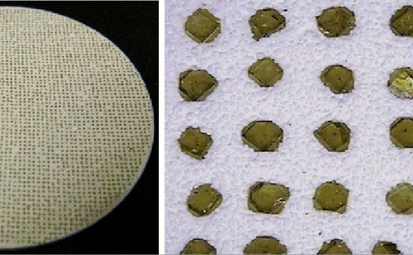
To obtain a large enough substrate on which to fabricate power-electronics devices, suppliers create larger-area substrates through a "tiling" process. This involves a mosaic of cut and polished single-crystal diamonds assembled into a tightly packed, flat array. Tiling is made possible via growth reactors that can produce 100-mm wafers.
“Scaling to this area for single wafers can be accomplished relatively painlessly, ” says eVince Technology (evincetechnology.com). “For practical applications, achieving high-yield production does not require a 100% defect-free substrate, so long as the wafer has a regular grid-iron pattern of high-quality areas of low-defect single-crystal diamond.”
Share this Post
latest post
-
 Semiconductor Processing November 26, 2023
 -
 Top Fabless Semiconductor companies October 27, 2023
 -
 Silicon Valley Semiconductor companies September 27, 2023
 -
 New Semiconductor companies August 28, 2023
 -
 List of Semiconductor companies in USA July 29, 2023
 -
 Semiconductor properties June 29, 2023
 -
 Semiconductor industry companies May 30, 2023
 -
 Canadian Semiconductor company April 30, 2023
 -
 Semiconductor companies in Europe March 31, 2023
 -
 Semiconductor jobs in Europe March 1, 2023
 -
 Freescale Semiconductor, Ltd January 30, 2023
 -
 Freescale Semiconductor Patent December 31, 2022
 -
 Freescale Semiconductor news December 1, 2022
 -
 Freescale Semiconductor stock symbol November 1, 2022
 -
 Global Semiconductor company October 28, 2022