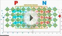
As an alternative to the Schottky Barrier contact described in the section Metal–Semiconductor Junction - Rectifying Contact, a junction between an n-type semiconductor and a p-type semiconductor can be used as a rectifying contact. To see why, browse through the animation below. The various parts of the animation are discussed in detail later in this section, so do not be concerned if you do not understand every stage. You can return to this animation as you read more about the p-n junction.
It should be noted in the above animation that the relative quantity of electrons in the p-type material and the relative quantity of holes in the n-type semiconductor before they are joined together has been greatly exaggerated for the purposes of illustration. Both of these are minority carriers in their respective environments – remember that electrons are the majority carriers in n-type semiconductors and that holes are the majority carriers in p-type semiconductors.
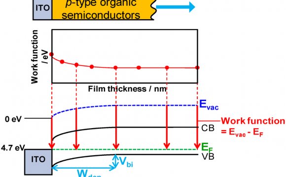
When the two semiconductors are initially joined together, electrons will flow from the n-type semiconductor into the p-type semiconductor, and holes will flow from the p-type semiconductor into the n-type semiconductor. The chemical potentials of the two semiconductors will come to equilibrium, and the band structures will be deformed accordingly. A depletion layer is formed at the interface between the two types of doped semiconductor, in which numbers of electrons in the conduction band and holes in the valence band are both significantly reduced.
RELATED VIDEO

Share this Post
latest post
-
 Semiconductor Processing November 26, 2023
 -
 Top Fabless Semiconductor companies October 27, 2023
 -
 Silicon Valley Semiconductor companies September 27, 2023
 -
 New Semiconductor companies August 28, 2023
 -
 List of Semiconductor companies in USA July 29, 2023
 -
 Semiconductor properties June 29, 2023
 -
 Semiconductor industry companies May 30, 2023
 -
 Canadian Semiconductor company April 30, 2023
 -
 Semiconductor companies in Europe March 31, 2023
 -
 Semiconductor jobs in Europe March 1, 2023
 -
 Freescale Semiconductor, Ltd January 30, 2023
 -
 Freescale Semiconductor Patent December 31, 2022
 -
 Freescale Semiconductor news December 1, 2022
 -
 Freescale Semiconductor stock symbol November 1, 2022
 -
 Global Semiconductor company October 28, 2022