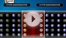
- Joining n-type material with p-type material causes excess electrons in the n-type material to diffuse to the p-type side and excess holes from the p-type material to diffuse to the n-type side.
- Movement of electrons to the p-type side exposes positive ion cores in the n-type side while movement of holes to the n-type side exposes negative ion cores in the p-type side, resulting in an electron field at the junction and forming the depletion region.
- A voltage results from the electric field formed at the junction.
P-n junctions are formed by joining -type and -type semiconductor materials, as shown below. Since the -type region has a high electron concentration and the -type a high hole concentration, electrons diffuse from the -type side to the -type side. Similarly, holes flow by diffusion from the -type side to the -type side. If the electrons and holes were not charged, this diffusion process would continue until the concentration of electrons and holes on the two sides were the same, as happens if two gasses come into contact with each other. However, in a p-n junction, when the electrons and holes move to the other side of the junction, they leave behind exposed charges on dopant atom sites, which are fixed in the crystal lattice and are unable to move. On the -type side, positive ion cores are exposed. On the -type side, negative ion cores are exposed. An electric field Ê forms between the positive ion cores in the -type material and negative ion cores in the -type material. This region is called the "depletion region" since the electric field quickly sweeps free carriers out, hence the region is depleted of free carriers. A "built in" potential Vbi due to Ê is formed at the junction. The animation below shows the formation of the Ê at the junction between and -type material.
RELATED VIDEO
