Need
Support?
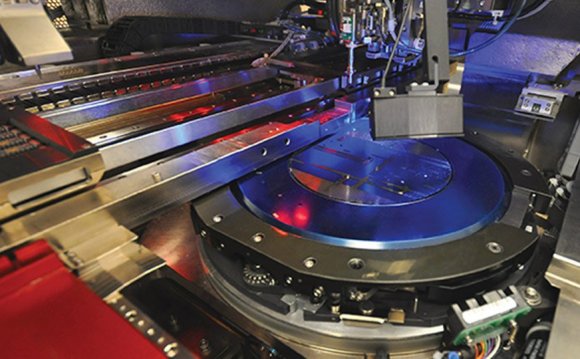
Manufacturing Facility

Wafer fab, assembly, and test operations with over 20, 000 square feet of clean room space, located on a 4.2 acre site with over 260, 000 square feet of building space.
- Fab: 6-inch
- Wafer Production: Interline Transfer, Full-Frame, and Linear CCD Image Sensors
- Assembly and Test: CCD and CMOS Image Sensors
- Acquired: Truesense Imaging, Inc. in April 2014
- Certifications:
- - ISO 9001:2008
Design Center
- Established: The Rochester Design Center’s roots go back to the early 1970’s, shortly after the CCD was invented, and was part of Eastman Kodak’s Physics Labs. In 2011, the Image Sensor Solutions business was spun off and became Truesense Imaging, Inc. ON Semiconductor obtained the design center through the acquisition of Truesense Imaging, Inc. in April, 2014.
- Focus End Markets: Medical, Industrial, Machine Vision, Surveillance, Intelligent Transportation Systems, Scientific Imaging
- Product Focus:CCD and CMOS Image Sensors
Source: www.onsemi.com
RELATED VIDEO

Download Optical Properties of Crystalline and Amorphous ...

Fundamentals of Semiconductors: Physics and Materials ...
Share this Post
latest post
-
 Semiconductor Processing November 26, 2023
 -
 Top Fabless Semiconductor companies October 27, 2023
 -
 Silicon Valley Semiconductor companies September 27, 2023
 -
 New Semiconductor companies August 28, 2023
 -
 List of Semiconductor companies in USA July 29, 2023
 -
 Semiconductor properties June 29, 2023
 -
 Semiconductor industry companies May 30, 2023
 -
 Canadian Semiconductor company April 30, 2023
 -
 Semiconductor companies in Europe March 31, 2023
 -
 Semiconductor jobs in Europe March 1, 2023
 -
 Freescale Semiconductor, Ltd January 30, 2023
 -
 Freescale Semiconductor Patent December 31, 2022
 -
 Freescale Semiconductor news December 1, 2022
 -
 Freescale Semiconductor stock symbol November 1, 2022
 -
 Global Semiconductor company October 28, 2022