By Jan Vardaman, TechSearch International, and Dan Tracy, SEMI
The electronics industry trend towards smaller and thinner form factors has ushered an era of significant changes in packaging materials. As these trends continue, innovative material solutions will be needed to address demanding requirements related to product integration, mobility, and reliability. Mobile electronics — especially smartphones and tablet computers — are the major unit volume drivers for semiconductor device sales and have unique packaging requirements. Given the compact form-factors and demands for connectivity, advanced packaging technologies such as wafer-level packaging (WLP), flip chip packaging for wireless, and package-on-package (PoP) deliver the necessary device integration needed in a thinner and smaller form factor package, and materials technologies are key in enabling this trend.
Flip Chip Package Growth Outlook
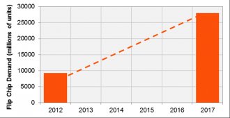
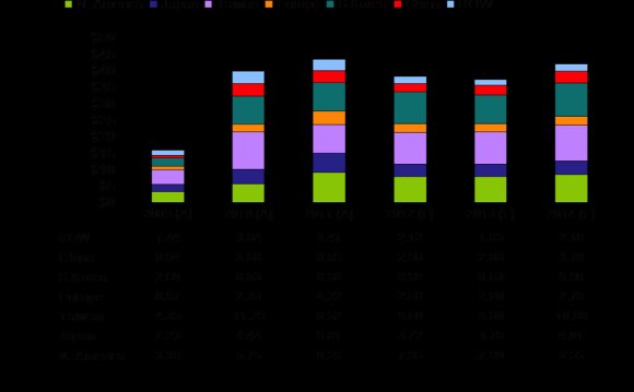
According to the upcoming SEMI Global Semiconductor Packaging Materials Outlook—2013-2014 Edition, the outlook for advanced packaging remains strong. These packages include ball grid array (BGA), CSP (including leadframe-based QFNs), flip chip, WLP, and various 3-D packages such as stacked-die and PoP. TechSearch has shown that 15 percent of 190 billion packaged ICs shipped in 2012 were in advanced packaging form factors, and this will grow to an estimated 21 percent of the 244 billion units to be shipped in 2017. Flip chip packaged units will grow at a compound annual growth rate (CAGR) of 25 percent between 2012 and 2017 with wireless products driving the growth. Over the same timeframe, WLP, which has already experience strong growth in unit shipments, is forecasted to grow at an 11 percent CAGR due to the strength in the mobile sector.
Advancements in materials technology and new materials will be needed to solve challenges pertaining to device and system integration and to package and system reliability. New materials and processes will enable the semiconductor industry to advance scaling in packaging down to the 16nm node and below. Semiconductor manufacturers and packaging subcontractors have identified a number of concerns, unmet material needs, and opportunities for material suppliers. The table below summarizes some general issues and topics identified particular material segment.
Key Issues and Concerns of Users of Packaging Materials
| Material Segment | Issues, Concerns, and Needs |
| Leadframes | - Concern about quality suppliers possibly exiting in market
- Limited sources for high pin count leadframe CSP - Longer lead times, especially for quick turn projects given limited investments by the suppliers |
| Organic Substrates | - Quality supplier base is available and it is geographically diversified |
RELATED VIDEO


Share this Post
latest post
-
 Semiconductor Processing November 26, 2023
 -
 Top Fabless Semiconductor companies October 27, 2023
 -
 Silicon Valley Semiconductor companies September 27, 2023
 -
 New Semiconductor companies August 28, 2023
 -
 List of Semiconductor companies in USA July 29, 2023
 -
 Semiconductor properties June 29, 2023
 -
 Semiconductor industry companies May 30, 2023
 -
 Canadian Semiconductor company April 30, 2023
 -
 Semiconductor companies in Europe March 31, 2023
 -
 Semiconductor jobs in Europe March 1, 2023
 -
 Freescale Semiconductor, Ltd January 30, 2023
 -
 Freescale Semiconductor Patent December 31, 2022
 -
 Freescale Semiconductor news December 1, 2022
 -
 Freescale Semiconductor stock symbol November 1, 2022
 -
 Global Semiconductor company October 28, 2022