 The manufacture of only silicon based semiconductors is described in this section; most semiconductors are silicon. Silicon is particularly suitable for integrated circuits because it readily forms an oxide coating, useful in patterning integrated components like transistors.
Silicon is the second most common element in the Earth’s crust in the form of silicon dioxide, SiO2, otherwise known as silica sand. Silicon is freed from silicon dioxide by reduction with carbon in an electric arc furnace
SiO2 + C = CO2+ Si
Such metalurgical grade silicon is suitable for use in silicon steel transformer laminations, but not nearly pure enough for semiconductor applications. Conversion to the chloride SiCl4 (or SiHCl3) allows purification by fractional distillation. Reduction by ultrapure zinc or magnesium yields sponge silicon, requiring further purification. Or, thermal decomposition on a hot polycrystalline silicon rod heater by hydrogen yields ultra pure silicon.
Si + 3HCl = SiHCl3 + H2 SiHCl3 + H2 = Si + 3HCl2
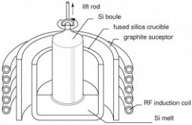
The polycrystalline silicon is melted in a fused silica crucible heated by an induction heated graphite suceptor. The graphite heater may alternately be directly driven by a low voltage at high current. In the Czochralski process, the silicon melt is solidified on to a pencil sized monocrystal silicon rod of the desired crystal lattice orientation. (Figure ) The rod is rotated and pulled upward at a rate to encourage the diameter to expand to several inches. Once this diameter is attained, the boule is automatically pulled at a rate to maintain a constant diameter to a length of a few feet. Dopants may be added to the crucible melt to create, for example, a P-type semiconductor. The growing apparatus is enclosed within an inert atmosphere.
Czochralski monocrystalline silicon growth.
The finished boule is ground to a precise final diameter, and the ends trimmed. The boule is sliced into wafers by an inside diameter diamond saw. The wafers are ground flat and polished. The wafers could have an N-type epitaxial layer grown atop the wafer by thermal deposition for higher quality. Wafers at this stage of manufacture are delivered by the silicon wafer manufacturer to the semiconductor manufacturer.
 Silicon boule is diamond sawed into wafers.
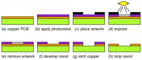
The processing of semiconductors involves photo lithography, a process for making metal lithographic printing plates by acid etching. The electronics based version of this is the processing of copper printed circuit boards. This is reviewed in Figure as an easy introduction to the photo lithography involved in semiconductor processing.
Processing of copper printed circuit boards is similar to the photo lithographic steps of semiconductor processing.
We start with a copper foil laminated to an epoxy fiberglass board in Figure (a). We also need positive artwork with black lines corresponding to the copper wiring lines and pads that are to remain on the finished board. Positive artwork is required because positive acting resist is used. Though, negative resist is available for both circuit boards and semiconductor processing. At (b) the liquid positive photo resist is applied to the copper face of the printed circuit board (PCB). It is allowed to dry and may be baked in an oven. The artwork may be a plastic film positive reproduction of the original artwork scaled to the required size. The artwork is placed in contact with the circuit board under a glass plate at (c). The board is exposed to ultraviolet light (d) to form a latent image of softened photo resist. The artwork is removed (e) and the softened resist washed away by an alkaline solution (f). The rinsed and dried (baked) circuit board has a hardened resist image atop the copper lines and pads that are to remain after etching. The board is immersed in the etchant (g) to remove copper not protected by hardened resist. The etched board is rinsed and the resist removed by a solvent.
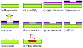 The major difference in the patterning of semiconductors is that a silicon dioxide layer atop the wafer takes the place of the resist during the high temperature processing steps. Though, the resist is required in low temperature wet processing to pattern the silicon dioxide.
An N-type doped silicon wafer in Figure (a) is the starting material in the manufacture of semiconductor junctions. A silicon dioxide layer (b) is grown atop the wafer in the presence of oxygen or water vapor at high temperature (over 1000o C in a diffusion furnace. A pool of resist is applied to the center of the cooled wafer, then spun in a vacuum chuck to evenly distribute the resist. The baked on resist (c) has a chrome on glass mask applied to the wafer at (d). This mask contains a pattern of windows which is exposed to ultraviolet light (e).
Manufacture of a silicon diode junction.
After the mask is removed in Figure (f), the positive resist can be developed (g) in an alkaline solution, opening windows in the UV softened resist. The purpose of the resist is to protect the silicon dioxide from the hydrofluoric acid etch (h), leaving only open windows corresponding to the mask openings. The remaining resist (i) is stripped from the wafer before returning to the diffusion furnace. The wafer is exposed to a gaseous P-type dopant at high temperature in a diffusion furnace (j). The dopant only diffuses into the silicon through the openings in the silicon dioxide layer. Each P-diffusion through an opening produces a PN junction. If diodes were the desired product, the wafer would be diamond scribed and broken into individual diode chips. However, the whole wafer may be processed further into bipolar junction transistors.
To convert the diodes into transistors, a small N-type diffusion in the middle of the existing P-region is required. Repeating the previous steps with a mask having smaller openings accomplishes this. Though not shown in Figure (j), an oxide layer was probably formed in that step during the P-diffusion.
The oxide layer over the P-diffusion is shown in Figure (k). Positive photo resist is applied and dried (l). The chrome on glass emitter mask is applied (m), and UV exposed (n). The mask is removed (o). The UV softened resist in the emitter opening is removed with an alkaline solution (p). The exposed silicon dioxide is etched away with hydrofluoric acid (HF) at (q)
Manufacture of a bipolar junction transistor, continuation of Manufacture of a silicon diode junction.
After the unexposed resist is stripped from the wafer (r), it is placed in a diffusion furnace (Figure (s) for high temperature processing. An N-type gaseous dopant, such phosphorus oxychloride (POCl) diffuses through the small emitter window in the oxide (s). This creates NPN layers corresponding to the emitter, base, and collector of a BJT. It is important that the N-type emitter not be driven all the way through the P-type base, shorting the emitter and collector. The base region between the emitter and collector also needs to be thin so that the transistor has a useful β. Otherwise, a thick base region could form a pair of diodes rather than a transistor. At (t) metalization is shown making contact with the transistor regions. This requires a repeat of the previous steps (not shown here) with a mask for contact openings through the oxide. Another repeat with another mask defines the metalization pattern atop the oxide and contacting the transistor regions through the openings.
The metalization could connect numerous transistors and other components into an integrated circuit. Though, only one transistor is shown. The finished wafer is diamond scribed and broken into individual dies for packaging. Fine gauge aluminum wire bonds the metalized contacts on the die to a lead frame, which brings the contacts out of the final package.
RELATED VIDEO


Share this Post
latest post
-
 Semiconductor Processing November 26, 2023
 -
 Top Fabless Semiconductor companies October 27, 2023
 -
 Silicon Valley Semiconductor companies September 27, 2023
 -
 New Semiconductor companies August 28, 2023
 -
 List of Semiconductor companies in USA July 29, 2023
 -
 Semiconductor properties June 29, 2023
 -
 Semiconductor industry companies May 30, 2023
 -
 Canadian Semiconductor company April 30, 2023
 -
 Semiconductor companies in Europe March 31, 2023
 -
 Semiconductor jobs in Europe March 1, 2023
 -
 Freescale Semiconductor, Ltd January 30, 2023
 -
 Freescale Semiconductor Patent December 31, 2022
 -
 Freescale Semiconductor news December 1, 2022
 -
 Freescale Semiconductor stock symbol November 1, 2022
 -
 Global Semiconductor company October 28, 2022