The increasing complexity of design enablement has prompted manufacturers to optimize the design process. New tools and techniques, thanks to next-generation hardware and software, have provided a new platform for semiconductor and wafer design. Advanced PDKs are the solution and have been developed by foundries to optimize the design process and leverage and reuse intellectual property (IP) and other general or specialized process building blocks. This article will explain what a PDK is, how it is implemented, and use the design rule constraints tool within the PKD, as the example.
What Are PDKs?
Process design kits consist of a set of files that typically contain descriptions of the basic building blocks of the process. They are expressed, algorithmically, as Pcells. These descriptions are stored in standardized Pcells libraries, design rules and rule constraints, schematics, SPICE model of transistors and other components, and layout information. They are used to describe, precisely, manufacturing process details for designers and design tools. The contents of the file will vary depending upon the target component, but they are all based upon the GDSII stream format.
PDK incarnations can involve any number of automated routine and rules. For example, arranging and routing programmable cells and analyzing the cell arrangement and interconnect wiring for optimum manufacturing. Other approaches can perform wire analysis and placement to prevent shorting. In other rules, the reliability of contacts and vias will be optimized by adding or subtracting additional metallization to the areas surrounding the contacts and vias. In still other cases, redundant contacts and vias may be adding to optimize efficiently manufacturability. Or, design and layout improvements can be made to cells in an iterative fashion.
PDKs will vary depending upon the specific device itself and their respective models. PDKs are generally specific to each foundry and the specific project or technology. Advanced PDKs contain specialized or proprietary data and/or functions, as well. The large foundries can offer a front-to-back integrated custom design environment that supports all major electronic data (EDA) vendors’ design flows. The major vendors include Synopsys, Lorenz Solutions, Helic, Cadence, Mentor Graphics, Ansys-Apache, and others.
The reason that PDKs have become the de-facto design approach to today’s semiconductor design is due to the complexities and ever-shrinking, ever-denser designs of new component technology. In a nutshell, PDKs automatically do the modifying and verification of the design modifications of complex semiconductor designs. This has antiquated the traditional top-down approach in favor of a new “parallel bottoms-up” verification approach that PDKs implement.
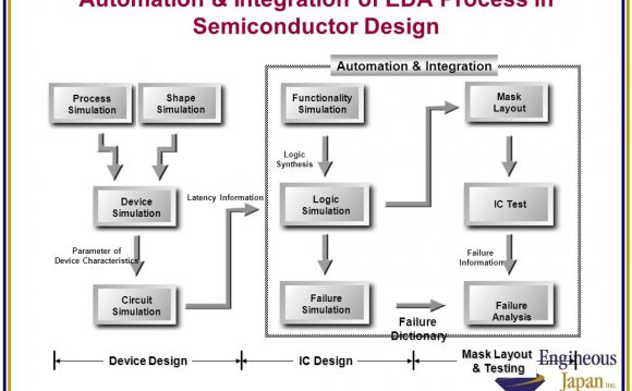
High Level Overview – How They Work
The PDKs make, and store, a “representation” for each of the components. This representation is defined by standard rules such as the minimum channel length of the transistor, well-to-well spacing, minimum metal width and metal to metal spacing, electrostatic discharge (ESD) and I/O rules. The automatic constraints of the area and perimeter of the diffusion of applicable components, setting limits for min and max feature sizes and verifying hotspots can be part of the representation, as well.
The PDKs purpose is to automatically adjust, depending on the data of the parameters stored in the file, the design layout for producibility and manufacturability. For example, if a particular PKD design rule is applied to the contact area, if it is made larger by the designer, the particular design rule constraint (DRC) for this component may instruct additional contact openings to be created, some others removed, or existing or new resized, etc. Exactly how this is implemented is defined in the specific PDK. The PDK will also automatically set these constraints for the designer and will allow only certain parameters to be varied during the evaluation of designs. Again it depends upon the specific parameters of the definitions within the particular PDK. The advantage of this approach is that the final designs are guaranteed to be perfectly compatible with the manufacturing process. This streamlines the design process, maximizing productivity and minimizing costs and providing the customer with a maximum value proposition.
In The Trenches – Comprehending Process Complexity
Today’s processes have become unfathomably complex. It is impossible for the designer to optimize, manually, semiconductor and other component design with any degree of efficiency. Today’s complex processes include functions such as double patterning, dual stress liners and double-exposure vias. This, in turn, has necessitated the need for an increasing number of design rules, which in turn, demands tighter uniformity control. All of this means that the post-layout verification is much more sophisticated, and cannot be verified without edge-of-the-envelope EDA software. Therefore, the only practical approach is to work with PDKs.
A typical PDK will have a number of modules that will be correlated with the PDK. These include
- Device models, which address shallow-trench isolation (STI), well proximity effect (WPE) and performance.
- Design for manufacturing (DFM) awareness, which implements design rule constraint (DRC), CFM Rules and Fill Generation
- Flow and Methodologies, which analyze and implement functional designs, verification and optimization and signoff for manufacturing.
- Lithography/OPC, which performs the hotspot verification, litho redesign and printability.
All of these modules have to be synchronized with the PDK, adding another level of complexity to the design flow. Today’s approach to PDKs is a different, more “holistic” integration where each peripheral process is optimized and synchronized to the specific technology or product design flow. And, has semiconductor parameters scale downward and densities increase, additional functions will be required to be integrated into the PDK.
An Example of an advanced PDK Element – Design Rule Constraints
Design rule constraints are one of the key processes in a PDK. Design rule constraints are the fundamental principles in constraining VLSI (Very Large Scale Integration) circuit designs to standardized physical and electrical manufacturability criterion.
Today’s component miniaturization and density technologies require continual reassessment of best-of-breed applications to keep design geometries aligned with realistic manufacturing capabilities. Even though two-dimensional DRC layout patterns may prove to be mathematically and layout rules compliant, when they are applied at the extremes of the manufacturing process tolerances, lithographic printability issues still arise.
Advanced DRCs are designed to identify 2D pattern anomalies during all stages of the design flow, not just in the early stages of the design process. Advanced DRCs function in the same fashion as traditional design constrained applications. However, it adds the function of associating a 2D pattern to each constraint, which acts as a filter to localize where the constraint is applied. This translates into, when the DRC tool is running, a DRC rule deck. It will enforce tighter constraints only where the anomalies occur. For this discussion, tip-to-side patterns are the subject.
RELATED VIDEO


Share this Post
latest post
-
 Semiconductor Processing November 26, 2023
 -
 Top Fabless Semiconductor companies October 27, 2023
 -
 Silicon Valley Semiconductor companies September 27, 2023
 -
 New Semiconductor companies August 28, 2023
 -
 List of Semiconductor companies in USA July 29, 2023
 -
 Semiconductor properties June 29, 2023
 -
 Semiconductor industry companies May 30, 2023
 -
 Canadian Semiconductor company April 30, 2023
 -
 Semiconductor companies in Europe March 31, 2023
 -
 Semiconductor jobs in Europe March 1, 2023
 -
 Freescale Semiconductor, Ltd January 30, 2023
 -
 Freescale Semiconductor Patent December 31, 2022
 -
 Freescale Semiconductor news December 1, 2022
 -
 Freescale Semiconductor stock symbol November 1, 2022
 -
 Global Semiconductor company October 28, 2022