Several major trends have been driving technological innovation in the display industry since its early days. These trends include image quality, screen size, portability and form factor. These have determined the direction of technological innovation and shaped entire value chains. The trends have in many cases resulted in a step change in technology, altering the value chain. This has, in turn, pushed many out of business while opening the door to others. The winners have been those who had bet on the right trend at the right time.
While these trends still remain strong undercurrents, new drivers are being introduced that will play a more prominent role in shaping the industry going forward. These new drivers will open up new frontiers, both on the technology and the market side. Indeed, they enable displays to both expand their existing markets and to diversify into new spaces.
These major drivers that are set to change the display landscape and technology include product differentiation, flexibility, 3D, transparency, system-on-panel, power savings, etc. As before, these trends have the potential to result in radical changes in technology, which would create opportunities and risks to all those exposed to the value chain of the display industry.
We will assess how these market trends will affect the choice of backplane technology and which backplane technology is likely to emerge as the winner.
Backplane technologies must adopt too
Interestingly, there are already many different backplane technologies that are mature and available, or are fast emerging. These include amorphous silicon, nanocrystalline silicon, low-temperature poly-silicon, solution-processed or evaporated organic semiconductor and various metal oxide thin film transistor technologies. Add to this multiplicity of solutions a range of emerging nano-systems (e.g., various nanowires, graphene, carbon nanotubes) and you will find a decision-making nightmare.
![]() This is because each thin film transistor technology offers a different set of characteristics, suitable for different needs. And yet none offers a one-size-fits-all-solution for all needs. This suggests that, at least initially, many different technologies will co-exist, each rising to satisfy a fragment of the emerging spectrum of needs and thus each occupying a different niche.
This is because each thin film transistor technology offers a different set of characteristics, suitable for different needs. And yet none offers a one-size-fits-all-solution for all needs. This suggests that, at least initially, many different technologies will co-exist, each rising to satisfy a fragment of the emerging spectrum of needs and thus each occupying a different niche.
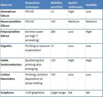
The table below outlines key parameters of several thin film deposition techniques. It assesses them on parameters such as deposition technique, mobility, spatial uniformity and temporal stability. These attributes will determine how each technology will ultimately fit within the changing display industry.
Table 1. Key parameters of thin-film deposition techniques
Amorphous silicon backplane is a winner when it comes to large-sized LCDs. It is amorphous therefore spatial uniformity is not an issue. The industry, as a whole, also has significant experience in using PECVDs for large-area deposition. The synergy with the a-Si photovoltaic technology also helps. The material can also be made thin and can also be transferred off glass and onto flexible substrate, introducing flexibility. The technology however fails when it comes to 3D, higher on-board processing power, and large-sized OLEDs. The limiting factor in all these aspects is the limited field-effect mobility.