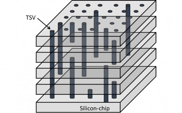
In electronic engineering, a through-silicon via (TSV) is a vertical electrical connection (via) passing completely through a silicon wafer or die. TSVs are a high performance interconnect technique used as an alternative to wire-bond and flip chips to create 3D packages and 3D integrated circuits, compared to alternatives such as package-on-package, because the density of the vias is substantially higher, and because the length of the connections is shorter.
Image sensors[edit]
CMOS image sensors (CIS) were among the first applications to adopt TSV(s) in volume manufacturing. In initial CIS applications, TSVs were formed on the backside of the image sensor wafer to form interconnects, eliminate wire bonds, and allow for reduced form factor and higher-density interconnects. Chip stacking only came about with the advent of backside illuminated (BSI) CIS, and involved reversing the order of the lens, circuitry, and photodiode from traditional front-side illumination so that the light coming through the lens first hits the photodiode and then the circuitry. This was accomplished by flipping the photodiode wafer, thinning the backside, and then bonding it on top of the readout layer using a direct oxide bond, with TSVs as interconnects around the perimeter.
3D packages[edit]
A 3D package (System in Package, Chip Stack MCM, etc.) contains two or more chips (integrated circuits) stacked vertically so that they occupy less space and/or have greater connectivity. An alternate type of 3D package can be found in IBM's Silicon Carrier Packaging Technology, where ICs are not stacked but a carrier substrate containing TSVs is used to connect multiple ICs together in a package. In most 3D packages, the stacked chips are wired together along their edges; this edge wiring slightly increases the length and width of the package and usually requires an extra “interposer” layer between the chips. In some new 3D packages, TSVs replace edge wiring by creating vertical connections through the body of the chips. The resulting package has no added length or width. Because no interposer is required, a TSV 3D package can also be flatter than an edge-wired 3D package. This TSV technique is sometimes also referred to as TSS (Through-Silicon Stacking or Thru-Silicon Stacking).
3D integrated circuits[edit]
A 3D integrated circuit (3D IC) is a single integrated circuit built by stacking silicon wafers and/or dies and interconnecting them vertically so that they behave as a single device. By using TSV technology, 3D ICs can pack a great deal of functionality into a small “footprint.” The different devices in the stack may be heterogeneous, e.g. combining CMOS logic, DRAM and III-V materials into a single IC. In addition, critical electrical paths through the device can be drastically shortened, leading to faster operation. The Wide I/O 3D DRAM memory standard (JEDEC JESD229) includes TSV in the design.
History of the term[edit]
The first TSV was patented by William Shockley in 1962, although most people in the electronics industry consider Merlin Smith and Emanuel Stern of IBM the inventors of TSV, based on their patent “Methods of Making Thru-Connections in Semiconductor Wafers” filed on December 28, 1964 and granted on September 26, 1967.
Share this Post
latest post
-
 Semiconductor Processing November 26, 2023
 -
 Top Fabless Semiconductor companies October 27, 2023
 -
 Silicon Valley Semiconductor companies September 27, 2023
 -
 New Semiconductor companies August 28, 2023
 -
 List of Semiconductor companies in USA July 29, 2023
 -
 Semiconductor properties June 29, 2023
 -
 Semiconductor industry companies May 30, 2023
 -
 Canadian Semiconductor company April 30, 2023
 -
 Semiconductor companies in Europe March 31, 2023
 -
 Semiconductor jobs in Europe March 1, 2023
 -
 Freescale Semiconductor, Ltd January 30, 2023
 -
 Freescale Semiconductor Patent December 31, 2022
 -
 Freescale Semiconductor news December 1, 2022
 -
 Freescale Semiconductor stock symbol November 1, 2022
 -
 Global Semiconductor company October 28, 2022