The ideal diode has zero resistance for the forward bias polarity, and infinite resistance (conducts zero current) for the reverse voltage polarity; if connected in an alternating current circuit, the semiconductor diode acts as an .
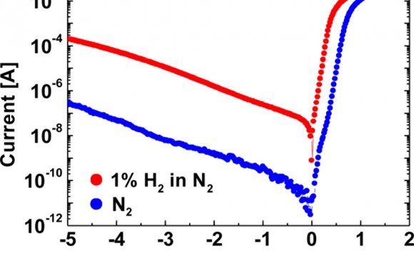
The semiconductor diode is not ideal. As shown in the figure, the diode does not conduct appreciably until a nonzero knee voltage (also called the turn-on voltage or the cut-in voltage) is reached. Above this voltage the slope of the current-voltage curve is not infinite (on-resistance is not zero). In the reverse direction the diode conducts a nonzero leakage current (exaggerated by a smaller scale in the figure) and at a sufficiently large reverse voltage below the breakdown voltage the current increases very rapidly with more negative reverse voltages.
As shown in the figure, the on and off resistances are the reciprocal slopes of the current-voltage characteristic at a selected bias point:
where rD is the resistance and ΔiD is the current change corresponding to the diode voltage change ΔvD at the bias vD=VBIAS.
Operation[edit]
Here, the operation of the abrupt p–n diode is considered. By "abrupt" is meant that the p- and n-type doping exhibit a step function discontinuity at the plane where they encounter each other. The objective is to explain the various bias regimes in the figure displaying current-voltage characteristics. Operation is described using band-bending diagrams that show how the lowest conduction band energy and the highest valence band energy vary with position inside the diode under various bias conditions. For additional discussion, see the articles Semiconductor and Band diagram.
Zero bias[edit]
The figure shows a band bending diagram for a p–n diode; that is, the band edges for the conduction band (upper line) and the valence band (lower line) are shown as a function of position on both sides of the junction between the -type material (left side) and the -type material (right side). When a -type and an -type region of the same semiconductor are brought together and the two diode contacts are short-circuited, the Fermi half-occupancy level (dashed horizontal straight line) is situated at a constant level. This level ensures that in the field-free bulk on both sides of the junction the hole and electron occupancies are correct. (So, for example, it is not necessary for an electron to leave the -side and travel to the -side through the short circuit to adjust the occupancies.)
Share this Post
latest post
-
 Semiconductor Processing November 26, 2023
 -
 Top Fabless Semiconductor companies October 27, 2023
 -
 Silicon Valley Semiconductor companies September 27, 2023
 -
 New Semiconductor companies August 28, 2023
 -
 List of Semiconductor companies in USA July 29, 2023
 -
 Semiconductor properties June 29, 2023
 -
 Semiconductor industry companies May 30, 2023
 -
 Canadian Semiconductor company April 30, 2023
 -
 Semiconductor companies in Europe March 31, 2023
 -
 Semiconductor jobs in Europe March 1, 2023
 -
 Freescale Semiconductor, Ltd January 30, 2023
 -
 Freescale Semiconductor Patent December 31, 2022
 -
 Freescale Semiconductor news December 1, 2022
 -
 Freescale Semiconductor stock symbol November 1, 2022
 -
 Global Semiconductor company October 28, 2022