Semiconductor diode theory is at the very centre of much of today's electronics industry. In fact semiconductor technology is present in almost every area of modern day technology and as such semiconductor theory is a very important element of electronics.
One of the fundamental structures within semiconductor technology is the PN junction. It is the fundamental building block of semiconductor diodes and transistors and a number of other electronic components.
The semiconductor diode has the valuable property that electrons only flow in one direction across it and as a result it acts as a rectifier. As it has two electrodes it receives its name - diode. In view of this, it is one of the most fundamental structures in semiconductor technology. Vast numbers of diodes are manufactured each year, and of course the semiconductor diode is the basis of many other devices apart from diodes. The bipolar junction transistor, junction FET and many more all rely on the PN junction for their operation. This makes the semiconductor PN junction diode one of the key enablers in today's electronics technology.
PN Junction
In its basic form a semiconductor diode is formed from a piece of silicon by making one end P type and the other end N type. This means that both ends have different characteristics. One end has an excess of electrons whilst the other has an excess of holes. Where the two areas meet the electrons fill the holes and there are no free holes or electrons. This means that there are no available charge carries in this region. In view of the fact that this area is depleted of charge carriers it is known as the depletion region.
The semiconductor diode PN junction with no bias appliedEven though the depletion region is very thin, often only few thousandths of a millimetre, current cannot flow in the normal way. Different effects are noticed dependent upon the way in which the voltage is applied to the junction. If the voltage is applied such that the P type area becomes positive and the N type becomes negative, holes are attracted towards the negative voltage and are assisted to jump across the depletion layer. Similarly electrons move towards the positive voltage and jump the depletion layer. Even though the holes and electrons are moving in opposite directions, they carry opposite charges and as a result they represent a current flow in the same direction.
The semiconductor diode PN junction with forward biasIf the voltage is applied to the semiconductor diode in the opposite sense no current flows. The reason for this is that the holes are attracted towards the negative potential that is applied to the P type region. Similarly the electrons are attracted towards the positive potential which is applied to the N type region. In other words the holes and electrons are attracted away from the junction itself and the depletion region increases in width. Accordingly no current flows.
The semiconductor diode PN junction with reverse biasPN junction characteristics
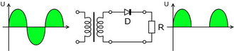
The PN junction is not an ideal rectifier diode having infinite resistance in the reverse direction and no resistance in the forward direction.
The characteristic of a diode PN junctionRELATED VIDEO


RELATED FACTS
-
 A rectifier is an electrical device that converts alternating current (AC), which periodically reverses direction, to direct current (DC), which flows in only one direction. The process is known as rectification. Physically, rectifiers take a number of forms...
- In electronics, an avalanche diode is a diode (made from silicon or other semiconductor) that is designed to go through avalanche breakdown at a specified reverse bias voltage. The junction of an avalanche diode is designed to prevent current concentration at hot...
- The Schottky diode (named after German physicist Walter H. Schottky; also known as hot carrier diode) is a semiconductor diode with a low forward voltage drop and a very fast switching action. The cat's-whisker detectors used in the early days of wireless can be...
Share this Post
latest post
-
 Semiconductor Processing November 26, 2023
 -
 Top Fabless Semiconductor companies October 27, 2023
 -
 Silicon Valley Semiconductor companies September 27, 2023
 -
 New Semiconductor companies August 28, 2023
 -
 List of Semiconductor companies in USA July 29, 2023
 -
 Semiconductor properties June 29, 2023
 -
 Semiconductor industry companies May 30, 2023
 -
 Canadian Semiconductor company April 30, 2023
 -
 Semiconductor companies in Europe March 31, 2023
 -
 Semiconductor jobs in Europe March 1, 2023
 -
 Freescale Semiconductor, Ltd January 30, 2023
 -
 Freescale Semiconductor Patent December 31, 2022
 -
 Freescale Semiconductor news December 1, 2022
 -
 Freescale Semiconductor stock symbol November 1, 2022
 -
 Global Semiconductor company October 28, 2022