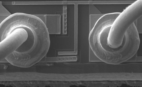
Delamination in semiconductor plastic packages often happens in many interfaces within the package itself, which is mainly caused by coefficient of thermal expansion (C.T.E) mismatch between the interfaces of two materials within the package. Die attach delamination is the separation between the silicon die and die attach pad on leadframe. Die attach delamination will reduce the total area of silicon die attached to pad and it is known to have increase the thermal resistance of the package. This could lead to early thermal shutdown of a device which uses exposed pad to dissipate heat. This paper is to investigate the die attach coverage effect on the package thermal resistance. A thermal modeling was done on various % of epoxy coverage to evaluate package thermal resistance. TQFP 100L with and without exposed pad are used for this model. Results show that die contact area to the pad will significantly affect the package thermal performance, especially at high power application. Package with exposed pad design will have higher increase of θja than non exposed pad in the event of die attach delamination.
RELATED VIDEO


Share this Post
latest post
-
 Semiconductor Processing November 26, 2023
 -
 Top Fabless Semiconductor companies October 27, 2023
 -
 Silicon Valley Semiconductor companies September 27, 2023
 -
 New Semiconductor companies August 28, 2023
 -
 List of Semiconductor companies in USA July 29, 2023
 -
 Semiconductor properties June 29, 2023
 -
 Semiconductor industry companies May 30, 2023
 -
 Canadian Semiconductor company April 30, 2023
 -
 Semiconductor companies in Europe March 31, 2023
 -
 Semiconductor jobs in Europe March 1, 2023
 -
 Freescale Semiconductor, Ltd January 30, 2023
 -
 Freescale Semiconductor Patent December 31, 2022
 -
 Freescale Semiconductor news December 1, 2022
 -
 Freescale Semiconductor stock symbol November 1, 2022
 -
 Global Semiconductor company October 28, 2022