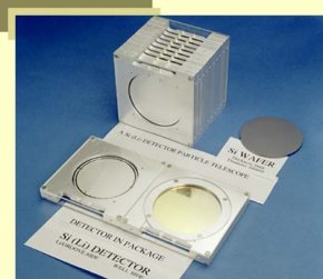
 Figure 2. A 100 mm diameter wafer and fabricated lithium-drifted Si detectors for the Cosmic Ray Isotope Spectrometer (CRIS) on NASA's Advanced Composition Explorer (ACE) spacecraft launched in 1997.
High-resistivity silicon detectors:
Detector arrays fabricated on high-resistivity Si wafers are being developed for a variety of applications, such as x-ray spectrometers for high-count-rate synchrotron radiation detection, portable instrumentation, and planetary exploration. Photodiode arrays are also being developed for medical imaging applications. The common feature of these devices is their extremely low noise, which results from the use of high-resistivity Si substrates and a low-leakage-current fabrication process that was originally developed for producing Si strip detectors for high-energy physics applications.
Fully-depleted silicon charge coupled devices:
Fully-depleted charge coupled devices (CCDs) are being developed for astronomy and astrophysics applications. Unlike conventional CCDs, which have a thin depletion layer only about 20 microns thick, fully depleted CCDs use high-resistivity Si and a substrate bias voltage to achieve full depletion of their 300-micron wafer thickness. This increased thickness translates into significantly higher quantum efficiency in the near infrared as well as in x-rays out to 20 keV or more.
 Because the device is fully depleted, it is sensitive to radiation absorbed at the back surface. This results in high sensitivity in the blue region of the spectrum without the need for the expensive back thinning process that is employed with conventional CCDs. For more information on fully-depleted CCDs, please visit .
Germanium detectors:
The current focus of the SDG in the Ge detector area is in the development and production of detectors with segmented electrodes fabricated using the SDG-developed amorphous-semiconductor electrical contact technology. This technology offers the advantages of: excellent energy resolution, potentially high spatial resolution, large active volumes leading to high detector efficiencies, simplified fabrication, and enabling unique detector geometries and detection schemes. Application areas for these detectors include gamma-ray astronomy, medical imaging, environmental remediation, x-ray spectroscopy using synchrotron radiation, nuclear physics, and nuclear material detection.
![]() Figure 3. A 25 by 25 orthogonal-strip Ge detector for gamma-ray imaging and high-resolution spectroscopy measurements. The active part of the detector is 60 mm by 60 mm by 10 mm thick and was produced using the amorphous-semiconductor electrical contact technology. The three-dimensional position and deposited energy for each gamma-ray interaction in such a detector can be accurately measured.
Figure 3. A 25 by 25 orthogonal-strip Ge detector for gamma-ray imaging and high-resolution spectroscopy measurements. The active part of the detector is 60 mm by 60 mm by 10 mm thick and was produced using the amorphous-semiconductor electrical contact technology. The three-dimensional position and deposited energy for each gamma-ray interaction in such a detector can be accurately measured.
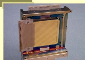
Figure 4. A 40 by 40 pixel array Ge detector developed for hard x-ray astronomy. The pixels are 0.3 mm by 0.3 mm in size with a 0.5 mm center-to-center spacing. The detector was produced using the amorphous- semiconductor electrical contact technology.
Cadmium zinc telluride detectors:
The current focus of the SDG in the CdZnTe detector area is in the development of compact, field-portable spectroscopy systems based on coplanar-grid detectors. The coplanar-grid technique was invented by the SDG and enables high spectral resolution combined with high detection efficiency. Currently, the SDG is developing these detectors for nuclear safeguard applications. Other potential applications include environmental remediation, well logging, medical diagnostics, and gamma-ray astronomy.
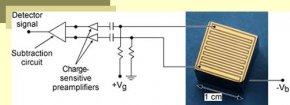 Figure 5. Photograph of a coplanar-grid CdZnTe gamma-ray detector combined with a schematic diagram of the front-end measurement electronics.
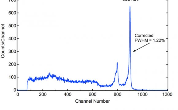
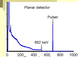
Figure 6. Measured 137Cs spectrum obtained with a 1 cm3 CdZnTe-based detector. Left: conventional planar geometry. Right: Coplanar-grid geometry. This demonstrates the spectroscopic performance improvement achieved with the coplanar-grid technique.
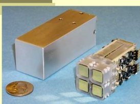
Figure 7. A 2 by 2 detector array assembled from four detector modules. Each module consists of a front-end electronics assembly and a 1 cm3 coplanar-grid CdZnTe detector contained in a compliant mount. Large detector arrays can be formed in this fashion in order to achieve the high detection efficiencies required in some applications.
Contact:
|
Lithium-drifted and high-resistivity silicon detectors:
|
|
|
Craig Tindall, Engineer
Phone: (510) 486-6523 E-mail: |
Paul Luke, Engineer
Phone: (510) 486-4962 E-mail: |
|
Fully-depleted silicon charge coupled devices:
|
|
|
Steve Holland, Engineer
Phone: (510) 486-5069 E-mail: |
|
|
Cadmium zinc telluride and Germanium detectors:
|
|
|
Paul Luke, Engineer
Phone: (510) 486-4962 E-mail: |
Mark Amman, Engineer
Phone: (510) 486-5638 E-mail: |
| MS 70A3362 | |
RELATED VIDEO

RELATED FACTS
-
This article is about particle detectors. For information about semiconductor detectors in radio, see Diode#Semiconductor_diodes, rectifier, detector (radio) and cat's-whisker detector.
A semiconductor detector is a device that uses a semiconductor (usually silicon...
Share this Post
latest post
-
 Semiconductor Processing November 26, 2023
 -
 Top Fabless Semiconductor companies October 27, 2023
 -
 Silicon Valley Semiconductor companies September 27, 2023
 -
 New Semiconductor companies August 28, 2023
 -
 List of Semiconductor companies in USA July 29, 2023
 -
 Semiconductor properties June 29, 2023
 -
 Semiconductor industry companies May 30, 2023
 -
 Canadian Semiconductor company April 30, 2023
 -
 Semiconductor companies in Europe March 31, 2023
 -
 Semiconductor jobs in Europe March 1, 2023
 -
 Freescale Semiconductor, Ltd January 30, 2023
 -
 Freescale Semiconductor Patent December 31, 2022
 -
 Freescale Semiconductor news December 1, 2022
 -
 Freescale Semiconductor stock symbol November 1, 2022
 -
 Global Semiconductor company October 28, 2022