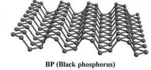
 Atomic structure of black phosphorus monolayer. Credit: Institute For Basic Science
Silicon Valley in Northern California got its nickname from the multitude of computer chip manufacturers that sprung up in the surrounding area in the 1980's. Despite its ubiquity as a chip building material, silicon may be facing some competition from a new version of an old substance.
Researchers working at the Institute for Basic Science (IBS) Center for Integrated Nanostructure Physics at Sungkyunkwan University (SKKU) in South Korea, led in part by Director Young Hee Lee, have created a high performance transistor using black phosphorus (BP) which has revealed some fascinating results.
Transistors are made up of materials with semiconducting properties, which come in two varieties: n-type (excess electrons) and p-type (excess holes). With the BP crystal, researchers have discovered that they can change its thickness and/or the contact metals and that will determine if it is high performance n-type, p-type, or ambipolar (function as both n- or p-type) material.
What does this mean?
Silicon has to be extrinsically doped (inserting another element into its crystal structure) to make it n-type or p-type in order for it to work in a semiconductor chip. The BP crystals can operate as both n-type and p-type or something in between, but don't require extrinsic doping. This means that instead of having to fabricate a silicon-arsenic crystal sandwiched between silicon-boron crystals, a transistor can have a single, lightweight, pure black phosphorus logic chip—no doping required.
Additionally, changing the metals used to connect the chip to the circuit has an influence on whether BP will be n- or p-type. Instead of doping to make an n- and p-type material, both n- and p-type BP can be put all together on one chip just by changing its thickness and the contact metal used.
Why is this important?
Technology manufacturers are in an arms race to make their devices lighter, smaller and more efficient. By using BP that is only several atomic layers thick, transistors can be made smaller and more energy efficient than what exists now.
Silicon chips exist in all of our electronic devices, and as manufacturers make devices smaller and more energy efficient, they begin to approach the threshold for just how small components can be. BP may provide a thinner, more efficient alternative to silicon chips in electrical devices.
Another example is tiny autonomous data recording and transmitting devices which will make up the Internet of Things (IoT). A major constraint from preventing IoT from taking off immediately is the inability to scale down the component size and the lack of a long-term power solution. 2 dimensional layered materials (such as black phosphorus) are interesting in this aspect, since both the electrical and mechanical properties are often enhanced compared to their bulk (3 dimensional) counterparts.
The atomic structure of black phosphorus and np-type transistor property of BP transistor. Credit: Institute For Basic ScienceIs BP a good alternative to current semiconductor materials?
It is a great material for transistors since it has a high carrier mobility (how quickly an electron can move through it). This gives BP the ability to operate at lower voltages while also increasing performance, which translates to greatly reduced power consumption.
With aluminum as a contact, thicker BP flakes (13 nanometer) show ambipolar properties similar to graphene while thin 3 nm flakes are unipolar n-type with switching on/off ratios greater than 105. The thinner they can make the material, the better the switching performance.
Perello explains, "The driving force in back phosphorus is the carrier mobility. Everything centers around that. The fact that the band gap changes with thickness also gives us flexibility in circuit design. As a researcher it gives me a lot of things to play with."
RELATED VIDEO

