Including Barrier Height Calculator
and
Depletion Width Calculator
Expand all / Compress all
Background
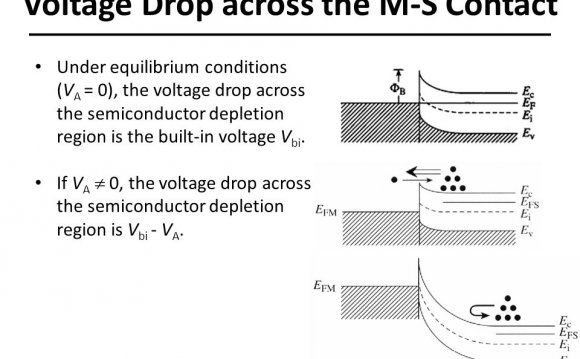
Whenever a metal and a semiconductor are in intimate contact, there exists a potential barrier between the two that prevents most charge carriers (electrons or holes) from passing from one to the other. Only a small number of carriers have enough energy to get over the barrier and cross to the other material. When a bias is applied to the junction, it can have one of two effects: it can make the barrier appear lower from the semiconductor side, or it can make it appear higher. The bias does not change the barrier height from the metal side.
The result of this is a Schottky Barrier (rectifying contact), where the junction conducts for one bias polarity, but not the other. Almost all metal-semiconductor junctions will exhibit some of this rectifying behavior.
Schottky Contacts make good diodes, and can even be used to make a kind of transistor, but for getting signals into and out of a semiconductor device, we generally want a contact that is Ohmic. Ohmic contacts conduct the same for both polarities. (They obey Ohm's Law).
There are two ways to make a metal-semiconductor contact look ohmic enough to get signals into and out of a semiconductor (or doing the opposite makes a good Schottky contact).
- Lower the barrier height
The barrier height is a property of the materials we use. We try to use materials whose barrier height is small.
Annealing can create an alloy between the semiconductor and the metal at the junction, which can also lower the barrier height. - Make the barrier very narrow
One very interesting property of very tiny particles like electrons and holes is that they can "tunnel" through barriers that they don't have enough energy to just pass over. The probability of tunneling becomes high for extremely thin barriers (in the tens of nanometers).
We make the barrier very narrow by doping it very heavily (1019 dopant atoms/cm3 or more).
Metal-Semiconductor Barrier Height Calculator
Select a metal: NOTE: The majority of the values obtained for the work functions of the elements above were found from this publication:
"The work function of the elements and its periodicity", Herbert B. Michaelson, Journal of Applied Physics 48, 4729-4733, (1977).
RELATED VIDEO


Share this Post
latest post
-
 Semiconductor Processing November 26, 2023
 -
 Top Fabless Semiconductor companies October 27, 2023
 -
 Silicon Valley Semiconductor companies September 27, 2023
 -
 New Semiconductor companies August 28, 2023
 -
 List of Semiconductor companies in USA July 29, 2023
 -
 Semiconductor properties June 29, 2023
 -
 Semiconductor industry companies May 30, 2023
 -
 Canadian Semiconductor company April 30, 2023
 -
 Semiconductor companies in Europe March 31, 2023
 -
 Semiconductor jobs in Europe March 1, 2023
 -
 Freescale Semiconductor, Ltd January 30, 2023
 -
 Freescale Semiconductor Patent December 31, 2022
 -
 Freescale Semiconductor news December 1, 2022
 -
 Freescale Semiconductor stock symbol November 1, 2022
 -
 Global Semiconductor company October 28, 2022