In most pure semiconductors at room temperature, the population of thermally excited charge carriers is very small. Often the concentration of charge carriers may be orders of magnitude lower than for a metallic conductor. For example, the number of thermally excited electrons cm–3 in silicon (Si) at 298 K is 1.5 × 10¹⁰. In gallium arsenide (GaAs) the population is only 1.1 × 10⁶ electrons cm–3. This may be compared with the number density of free electrons in a typical metal, which is of the order of 1028 electrons cm–3.
Given these numbers of charge carriers, it is no surprise that, when they are extremely pure, silicon and other semiconductors have high electrical resistivities, and therefore low electrical conductivities. This problem can be overcome by doping a semiconducting material with impurity atoms. Even very small controlled additions of impurity atoms at the 0.0001% level can make very large differences to the conductivity of a semiconductor.
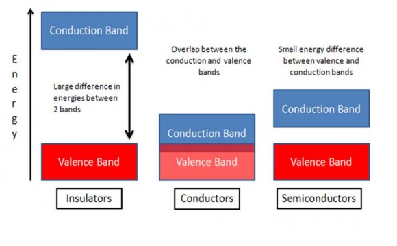
It is easiest to begin with a specific example. Silicon is a group IV element, and has 4 valence electrons per atom. In pure silicon the valence band is completely filled at absolute zero. At finite temperatures the only charge carriers are the electrons in the conduction band and the holes in the valence band that arise as a result of the thermal excitation of electrons to the conduction band. These charge carriers are called intrinsic charge carriers, and necessarily there are equal numbers of electrons and holes. Pure silicon is therefore an example of an intrinsic semiconductor.
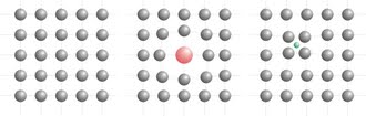
If a very small number of atoms of a group V element such as phosphorus (P) are added to the silicon as substitutional atoms in the lattice, additional valence electrons are introduced into the material because each phosphorus atom has 5 valence electrons. These additional electrons are bound only weakly to their parent impurity atoms (the bonding energies are of the order of hundredths of an eV), and even at very low temperatures these electrons can be promoted into the conduction band of the semiconductor. This is often represented schematically in band diagrams by the addition of 'donor levels' just below the bottom of the conduction band, as in the schematic below.
The presence of the dotted line in this schematic does not mean that there now exist allowed energy states within the band gap. The dotted line represents the existence of additional electrons which may be easily excited into the conduction band. Semiconductors that have been doped in this way will have a surplus of electrons, and are called -type semiconductors. In such semiconductors, electrons are the majority carriers.
Conversely, if a group III element, such as aluminium (Al), is used to substitute for some of the atoms in silicon, there will be a deficit in the number of valence electrons in the material. This introduces electron-accepting levels just above the top of the valence band, and causes more holes to be introduced into the valence band. Hence, the majority charge carriers are positive holes in this case. Semiconductors doped in this way are termed p-type semiconductors.
Doped semiconductors (either -type or p-type) are known as extrinsic semiconductors. The activation energy for electrons to be donated by or accepted to impurity states is usually so low that at room temperature the concentration of majority charge carriers is similar to the concentration of impurities. It should be remembered that in an extrinsic semiconductor there is an contribution to the total number of charge carriers from intrinsic electrons and holes, but at room temperature this contribution is often very small in comparison with the number of charge carriers introduced by the controlled impurity doping of the semiconductor.
RELATED VIDEO

RELATED FACTS
-
 In semiconductor production, doping intentionally introduces impurities into an extremely pure (also referred to as intrinsic) semiconductor for the purpose of modulating its electrical properties. The impurities are dependent upon the type of semiconductor. Lightly...
-
An extrinsic semiconductor is a semiconductor that has been doped, that is, into which a doping agent has been introduced, giving it different electrical properties than the intrinsic (pure) semiconductor.
Doping involves adding dopant atoms to an intrinsic... - A dopant, is also called a doping agent, is a trace impurity element that is inserted into a substance (in very low concentrations) in order to alter the electrical properties or the optical properties of the substance. In the case of crystalline substances, the...
Share this Post
latest post
-
 Semiconductor Processing November 26, 2023
 -
 Top Fabless Semiconductor companies October 27, 2023
 -
 Silicon Valley Semiconductor companies September 27, 2023
 -
 New Semiconductor companies August 28, 2023
 -
 List of Semiconductor companies in USA July 29, 2023
 -
 Semiconductor properties June 29, 2023
 -
 Semiconductor industry companies May 30, 2023
 -
 Canadian Semiconductor company April 30, 2023
 -
 Semiconductor companies in Europe March 31, 2023
 -
 Semiconductor jobs in Europe March 1, 2023
 -
 Freescale Semiconductor, Ltd January 30, 2023
 -
 Freescale Semiconductor Patent December 31, 2022
 -
 Freescale Semiconductor news December 1, 2022
 -
 Freescale Semiconductor stock symbol November 1, 2022
 -
 Global Semiconductor company October 28, 2022