Silicon is a chemical element with the symbol Si and atomic number 14. It is less reactive than its chemical analog carbon, the nonmetal directly above it in the periodic table, but more reactive than germanium, the metalloid directly below it in the table. Silicon is the eighth most common element in the universe by mass, but very rarely occurs as the pure free element in nature. It is most widely distributed in dusts, sands, planetoids, and planets as various forms of silicon dioxide (silica) or silicates. Silicon is the second most abundant element in the Earth's crust.
Elemental silicon also has a large impact on the modern world economy. Although most free silicon is used in the steel refining, aluminum-casting, and fine chemical industries, the relatively small portion (
Silicon chips are the basis of modern electronic and computing. The silicon must be ultrapure, although depending on final use it may be doped with part per million levels of arsenic, boron, gallium, germanium, or phosphorus.
Electronic Grade
The use of silicon in semiconductor devices requires a much higher purity than metallurgical grade silicon. Very pure silicon (>99.9%) can be extracted directly from solid silica or other silicon compounds by molten salt electrolysis. This method, known as early as 1854, has the potential to directly produce solar-grade silicon without any carbon dioxide emission at much lower energy consumption.
Bulk silicon wafers used in integrated circuits must first be refined to an even higher "nine nines" purity (%), a process which requires repeated applications of refining technology.
The majority of silicon crystals grown for IC device production are produced by the Czochralski process, (CZ-Si) since it is the least expensive method available and it is capable of producing large size crystals. In addition, a number of other methods have been used to produce even higher “ultra-high-purity” silicon.
Early silicon purification techniques were based on the fact that if silicon is melted and re-solidified, the last parts of the mass to solidify contain most of the impurities. The earliest method of silicon purification, involved crushing metallurgical grade silicon and then partially dissolving the silicon powder in an acid. When crushed, the silicon cracked so that the weaker impurity-rich regions were on the outside of the resulting grains of silicon. As a result, the impurity-rich silicon was the first to be dissolved when treated with acid, leaving behind a more pure product.
In zone melting, also called zone refining, the first silicon purification method to be widely used industrially, rods of metallurgical grade silicon are heated to melt at one end. Then, the heater is slowly moved down the length of the rod, keeping a small length of the rod molten as the silicon cools and re-solidifies behind it. Since most impurities tend to remain in the molten region rather than re-solidify, when the process is complete, most of the impurities in the rod will have been moved into the end that was the last to be melted. This end is then cut off and discarded, and the process repeated if a still higher purity is desired.
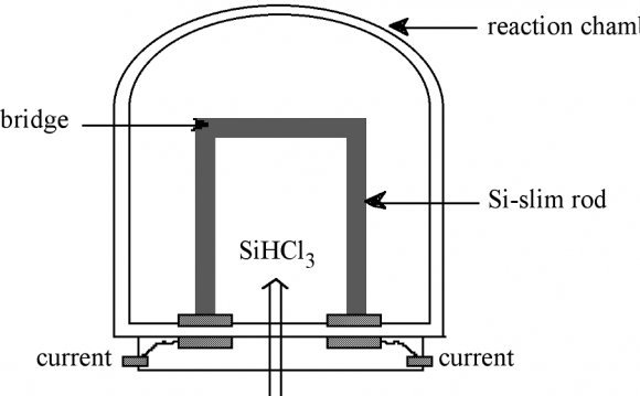
At one time, DuPont produced ultra-pure silicon by reacting silicon tetrachloride with high-purity zinc vapors at 950 °C, producing silicon by SiCl4 + 2 Zn → Si + 2 ZnCl2. However, this technique was plagued with practical problems (such as the zinc chloride byproduct solidifying and clogging lines) and was eventually abandoned in favor of the Siemens process. In the Siemens process, high-purity silicon rods are exposed to trichlorosilane at 1150 °C. The trichlorosilane gas decomposes and deposits additional silicon onto the rods, enlarging them because 2 HSiCl3 → Si + 2 HCl + SiCl4. Silicon produced from this and similar processes is called polycrystalline silicon. Polycrystalline silicon typically has impurity levels of less than one part per billion.
In 2006 REC announced construction of a plant based on fluidized bed (FB) technology using silane: 3 SiCl4 + Si + 2 H2 → 4 HSiCl3, 4 HSiCl3 → 3 SiCl4 + SiH4, SiH4 → Si + 2 H2. The advantage of fluid bed technology is that processes can be run continuously, yielding higher yields than Siemens Process, which is a batch process.
Today, silicon is purified by converting it to a silicon compound that can be more easily purified by distillation than in its original state, and then converting that silicon compound back into pure silicon. Trichlorosilane is the silicon compound most commonly used as the intermediate, although silicon tetrachloride and silane are also used. When these gases are blown over silicon at high temperature, they decompose to high-purity silicon.
Monocrystalline Silicon
 Single-crystal silicon is the primary substrate material of the microelectronics industry. It consists of silicon in which the crystal lattice of the entire solid is continuous, unbroken to its edges. It can be prepared intrinsic, i.e. made of exceedingly pure silicon alone, or doped, containing very small quantities of other elements added to change in a controlled manner its semiconducting properties. Most silicon monocrystals are grown by the Czochralski process, in the shape of cylinders up to 2 m long and 45 cm in diameter which when cut in thin slices, produces the wafers onto which the microcircuits will be fabricated.
Single-crystal silicon is possibly the most important technological material of the last decades (the "silicon era"), because it has been essential to the development of the electronic devices on which the present day electronic and information revolution is based.
Monocrystalline is different from amorphous silicon, in which the atomic order is limited to short range order only. In between the two extremes there is polycrystalline silicon, which is made up of small crystals, known as crystallites.
The monocrystalline form of silicon is used in the semiconductor device fabrication since grain boundaries would bring discontinuities and defects, which can have significant effects on the properties of the material. On the scale that devices operate on, these imperfections would have a significant impact on the functionality and reliability of the devices.
Monocrystalline silicon is also used in the manufacturing of high performance solar cells. However, since solar cells are less demanding than microelectronics, as far as structural imperfections are concerned, monocrystaline solar grade (Sog-Si) is often used, single crystal is also often replaced by the cheaper polycrystalline or multicrystalline silicon.
state education rankings 2020 blogging with wix education ranking us bill nye education nevada department of education dekalb county board of education can you make more money blogging or vlogging bibb county board of education blogging zarada shelby county board of education landmark education blog games getting into blogging environmental education blog.inside out-prison acs education blog pro amasty states by education public education ranking by state blogging to win course review examples of critical race theory in education soundtrap for education ny board of education relay graduate school of education blogging dirty blog jokes blog designers near me i am malala: how one girl stood up for education and changed the world blogging quiz claire till blog blogging rubric blogging about your personal life south carolina education lottery powerball blogging name ideas mac education discount global education blog names for lifestyle what do you mean by blog physical education blogging through the fourth dimension box tops for education blogging quotes affirmative action in education blogging dallas cowboys blogging under your own name what is rti in education blog sign off examples vlogging camera oklahoma department of education blog over 50 feeling 40 blogging guideShare this Post
latest post
-
 Semiconductor Processing November 26, 2023
 -
 Top Fabless Semiconductor companies October 27, 2023
 -
 Silicon Valley Semiconductor companies September 27, 2023
 -
 New Semiconductor companies August 28, 2023
 -
 List of Semiconductor companies in USA July 29, 2023
 -
 Semiconductor properties June 29, 2023
 -
 Semiconductor industry companies May 30, 2023
 -
 Canadian Semiconductor company April 30, 2023
 -
 Semiconductor companies in Europe March 31, 2023
 -
 Semiconductor jobs in Europe March 1, 2023
 -
 Freescale Semiconductor, Ltd January 30, 2023
 -
 Freescale Semiconductor Patent December 31, 2022
 -
 Freescale Semiconductor news December 1, 2022
 -
 Freescale Semiconductor stock symbol November 1, 2022
 -
 Global Semiconductor company October 28, 2022