Organic semiconductors are solids whose building blocks are pi bonded molecules or polymers made up by carbon and hydrogen atoms and – at times – heteroatoms such nitrogen, sulfur and oxygen. They exist in form of molecular crystals or amorphous thin films. In general, they are insulators but become semiconducting when charges are either injected from appropriate electrodes, upon doping or by photoexcitation.
General properties[edit]
In molecular crystals the energetic separation between the top of the valence band and the bottom conduction band, i.e. the band gap, is typically 2.5 – 4 eV while in inorganic semiconductors the band gaps are typically 1 – 2 eV. This implies that they are, in fact, insulators rather than semiconductors in the conventional sense. They become semiconducting only when charge carriers are either injected from the electrodes or generated via intentional or unintentional doping. Charge carriers can also be generated in the course of optical excitation. It is important to realize, however, that the primary optical excitations are neutral excitons with a Coulomb-binding energy of typically 0.5 – 1.0 eV. The reason is that in organic semiconductors their dielectric constants are as low as 3-4. This impedes efficient photogeneration of charge carriers in neat systems in the bulk. Efficient photogeneration can only occur in binary systems due to charge transfer between donor and acceptor moieties. Otherwise neutral excitons decay radiatively to the ground state - thereby emitting photoluminescence – or non-radiatively. The optical absorption edge of organic semiconductors is typically 1.7 – 3 eV, equivalent to a spectral range from 700 to 400 nm
History[edit]
The fact that organic semiconductors are, in principle, insulators but become semiconducting when charge carriers are injected from the electrode(s) was discovered by Kallmann and Pope. They found that a hole current can flow through an anthracene crystal contacted with a positively biased electrolyte containing iodine that can act as a hole injector. This work was stimulated by the earlier discovery by Akamatu et al. that aromatic hydrocarbons become conductive when blended with molecular iodine because a charge transfer complex is formed. Since it was readily realized that the crucial parameter that controls injection is the work-function of the electrode, it was straightforward to replace the electrolyte by a solid metallic or semiconducting contact with an appropriate work-function. When both electrons and holes are injected from opposite contacts they can recombine radiatively and emit electroluminescence. It was observed in organic crystals in 1965 by Sano et al.
This discovery paved the way for applying organic solids as active elements in semiconducting electronic devices, such as organic light emitting diodes (OLEDs) that rely on the recombination of electrons and hole injected from "ohmic"electrodes, i.e. electrodes with unlimited supply of charge carriers. The next major step towards the technological exploitation of the phenomenon of electron and hole injection into a non-crystalline organic semiconductor was the work by Tang and Van Slyke. They showed that efficient electroluminescence can be generated in an vapor-deposited thin amorphous bilayer of an aromatic diamine (TAPC) and Alq3 sandwiched between an indium-tin-oxide (ITO) anode and an Mg:Ag cathode. Another milestone towards the development or organic light emitting diodes (OLEDs) was the recognition that also conjugated polymers can be used as active materials. The efficiency of OLEDs was greatly improved when realizing that phosphorescent states (triplet excitons) may be used for emission when doping an organic semiconductor matrix with a phosphorescent dye, such as complexes of iridium with strong spin-orbit coupling.
In the course of their early work on conductivity of an anthracene crystal contacted with an electrolyte, Kallmann and Pope also found that an optically excited dye molecules adsorbed at the surface of the crystal can inject a charge carriers. The underlying phenomenon is called sensitized photoconductivity. It occurs when photo-exciting a dye molecule with appropriate oxidation/reduction potential adsorbed at the surface or incorporated in the bulk. This effect revolutionized electrophotography which is the technological basis of today’s office copying machines. It is also the basis of organic solar cells (OSCs) in which the active element is an electron donor and an electron acceptor material is combined in a bilayer or a bulk hetero junction.
Doping with strong electron donor or acceptors can render organic solids conductive even in the absence of light. Examples are doped polyacetylene and doped light emitting diodes.
Today organic semiconductors are used as active elements in organic light emitting diodes (OLEDs), organic solar cells (OSCs) and organic field effect transistors (OFETs).
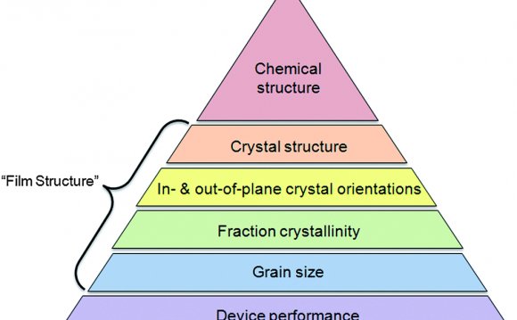
Amorphous molecular films[edit]
They are formed by depositing organic molecules through evaporation or spin-coating and are employed for device applications such as OLEDs. OFETs and OSCs.- Prototypical materials are Alq3, C60, phenyl-C61-butyric acid methyl ester (PCBM), pentacene, triphenyl diamin (TPD) derivaties of carbazole, phthalocyanine.
Molecularly doped polymers[edit]
They are prepared by spreading a film of an electrically inert polymer, e.g. polycarbonate, doped with typically 30% of charge transporting molecules, on top of a base electrode. Typical materials are members of the triphenylene family. They are used as photoreceptors in electrophotography. This requires films have a thickness of several micrometers that can be prepared using the doctor-blade technique.
Molecular crystals[edit]
In the early days of fundamental research into organic semiconductors the prototypical materials were free-standing single crystals of the acene family, e.g. anthracene and tetracene. The advantage of employing molecular crystals instead of amorphous film is that their charge carrier mobilities are much larger. This is of particular advantage for OFET applications. Examples are thin films of crystalline rubrene prepared by hot wall epitaxy.
Neat polymer films[edit]
They are usually processed from solution employing variable deposition techniques including simple spin-coating, ink-jet deposition or industrial reel-to-reel coating which allows preparing thin films on a flexible substrate. The materials of choice are conjugated polymers such as poly-thiophene, poly-phenylenevinylene, and copolymers of alternating donor and acceptor units such as members of the poly(carbazole-dithiophene-benzothiadiazole (PCDTBT) family. For solar cell applications they can be blended with C60 or PCBM are electron acceptors.
RELATED VIDEO
RELATED FACTS
-
 An organic semiconductor is an organic material with semiconductor properties. Single molecules, short chain (oligomers) and organic polymers can be semiconductive. Semiconducting small molecules (aromatic hydrocarbons) include the polycyclic aromatic compounds...
Share this Post
latest post
-
 Semiconductor Processing November 26, 2023
 -
 Top Fabless Semiconductor companies October 27, 2023
 -
 Silicon Valley Semiconductor companies September 27, 2023
 -
 New Semiconductor companies August 28, 2023
 -
 List of Semiconductor companies in USA July 29, 2023
 -
 Semiconductor properties June 29, 2023
 -
 Semiconductor industry companies May 30, 2023
 -
 Canadian Semiconductor company April 30, 2023
 -
 Semiconductor companies in Europe March 31, 2023
 -
 Semiconductor jobs in Europe March 1, 2023
 -
 Freescale Semiconductor, Ltd January 30, 2023
 -
 Freescale Semiconductor Patent December 31, 2022
 -
 Freescale Semiconductor news December 1, 2022
 -
 Freescale Semiconductor stock symbol November 1, 2022
 -
 Global Semiconductor company October 28, 2022