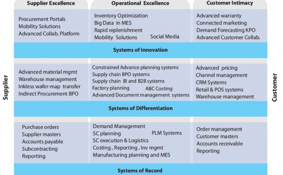
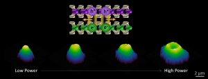
 Heterostructures formed by different three-dimensional semiconductors form the foundation for modern electronic and photonic devices. Now, University of Washington scientists have successfully combined two different ultrathin semiconductors — each just one layer of atoms thick and roughly 100, 000 times thinner than a human hair — to make a new two-dimensional heterostructure with potential uses in clean energy and optically-active electronics. The team, led by Boeing Distinguished Associate Professor Xiaodong Xu, announced its findings in a paper published Feb. 12 in the journal Science.
“What we’re seeing here is distinct from heterostructures made of 3-D semiconductors, ” said Xu, who has joint appointments in the Department of Physics and the Department of Materials Science and Engineering. “We’ve created a system to study the special properties of these atomically thin layers and their potential to answer basic questions about physics and develop new electronic and photonic technologies.”
When semiconductors absorb light, pairs of positive and negative charges can form and bind together to create so-called excitons. Scientists have long studied how these excitons behave, but when they are squeezed down to the 2-D limit in these atomically thin materials, surprising interactions can occur.
While traditional semiconductors manipulate the flow of electron charge, this device allows excitons to be preserved in “valleys, ” a concept from quantum mechanics similar to the spin of electrons. This is a critical step in the development of new nanoscale technologies that integrate light with electronics.
“It was already known that these ultrathin 2-D semiconductor have these unique properties that you cannot find in other 2-D or 3-D arrangements, ” said Xu. “But as we show here, when we put these two layers together — one on top of the other — the interface between these sheets becomes the site of even more new physical properties, which you don’t see in each layer on its own or in the 3-D version.”
Xu and his team wanted to create and explore the properties of a 2-D semiconductor heterostructure made up of two different layers of material, a natural expansion of their previous studies on atomically thin junctions, as well as nanoscale lasers based on atomically thin layers of semiconductors. By studying how laser light interacts with this heterostructure, they gathered information about the physical properties at the atomically sharp interface.
“Many groups have studied the optical properties of single 2-D sheets, ” said Seyler. “What we do here is carefully stack one material on top of another, and then study the new properties that arise at the interface.”
RELATED VIDEO

Share this Post
latest post
-
 Semiconductor Processing November 26, 2023
 -
 Top Fabless Semiconductor companies October 27, 2023
 -
 Silicon Valley Semiconductor companies September 27, 2023
 -
 New Semiconductor companies August 28, 2023
 -
 List of Semiconductor companies in USA July 29, 2023
 -
 Semiconductor properties June 29, 2023
 -
 Semiconductor industry companies May 30, 2023
 -
 Canadian Semiconductor company April 30, 2023
 -
 Semiconductor companies in Europe March 31, 2023
 -
 Semiconductor jobs in Europe March 1, 2023
 -
 Freescale Semiconductor, Ltd January 30, 2023
 -
 Freescale Semiconductor Patent December 31, 2022
 -
 Freescale Semiconductor news December 1, 2022
 -
 Freescale Semiconductor stock symbol November 1, 2022
 -
 Global Semiconductor company October 28, 2022