Please log in to see this content.
You have no subscription access to this content.
No metrics data to plot.
The attempt to load metrics for this article has failed.
The attempt to plot a graph for these metrics has failed.
The full text of this article is not currently available.
Noncontact semiconductor wafer characterization with the terahertz Hall effect
Abstract
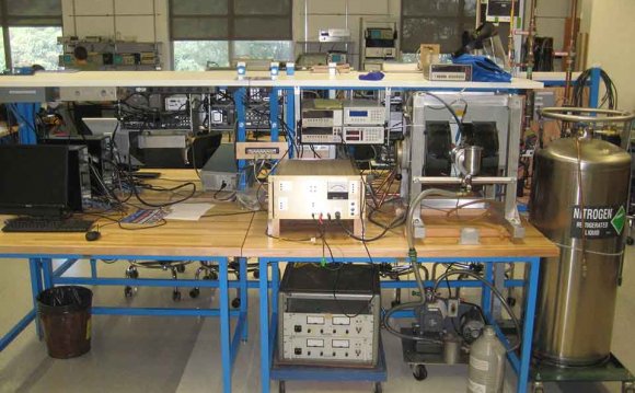
We demonstrate noncontact measurements of the Hall mobility of dopedsemiconductor wafers with roughly 250 μm spatial resolution, using polarization rotation of focused beams of terahertz (THz) radiation in the presence of a static magnetic field. Quantitative and independent images of both carrier density and mobility of a dopedsemiconductor wafer have been obtained.
© 1997 American Institute of Physics
Received Thu Dec 19 00:00:00 UTC 1996 Accepted Mon May 26 00:00:00 UTC 1997
/content/aip/journal/apl/71/1/10.1063/1.119456
Article metrics loading...
Full text loading...
RELATED VIDEO

Share this Post
latest post
-
 Semiconductor Processing November 26, 2023
 -
 Top Fabless Semiconductor companies October 27, 2023
 -
 Silicon Valley Semiconductor companies September 27, 2023
 -
 New Semiconductor companies August 28, 2023
 -
 List of Semiconductor companies in USA July 29, 2023
 -
 Semiconductor properties June 29, 2023
 -
 Semiconductor industry companies May 30, 2023
 -
 Canadian Semiconductor company April 30, 2023
 -
 Semiconductor companies in Europe March 31, 2023
 -
 Semiconductor jobs in Europe March 1, 2023
 -
 Freescale Semiconductor, Ltd January 30, 2023
 -
 Freescale Semiconductor Patent December 31, 2022
 -
 Freescale Semiconductor news December 1, 2022
 -
 Freescale Semiconductor stock symbol November 1, 2022
 -
 Global Semiconductor company October 28, 2022