A P-type semiconductor is an intrinsic semiconductor (like Si) in which an impurity acting as an acceptor (like e.g. boron B in Si) has been intentionally added. These impurities are called acceptors since once they are inserted in the crystalline lattice, they lack one or several electrons to realize a full bonding with the rest of the crystal.
Figure 5 : schematic representation of a Si crystal doped with boron (B)
From figure 5, we see that a p-type semiconductor has a lower electron density n and a higher hole density p than the same intrinsic semiconductor. Electrons are said to be the minority carriers whereas holes are the majority carriers.
For extrinsic semiconductors, the dopant density is always far higher than the intrinsic carrier density : NA>ni. In the case of a p-type material, the hole density is then close to the dopant density NA. Since the law of mass action is always true, we obtain the following expressions for the carrier densities
The Fermi level for a p-type semiconductor or chemical potential is then :
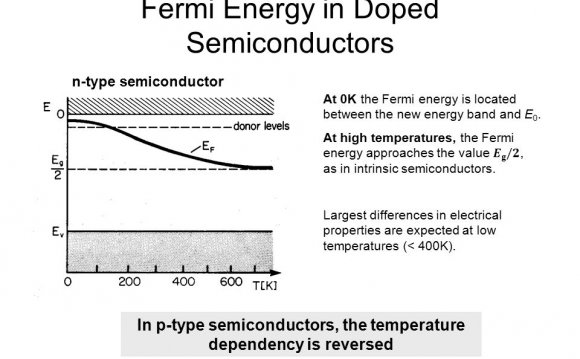
When the acceptor density is increased, the Fermi level moves closer to the edge of the valence band. If NA=Nv the Fermi level enters the valence band, the semiconductor is then said to be degenerate.
RELATED VIDEO


Share this Post
latest post
-
 Semiconductor Processing November 26, 2023
 -
 Top Fabless Semiconductor companies October 27, 2023
 -
 Silicon Valley Semiconductor companies September 27, 2023
 -
 New Semiconductor companies August 28, 2023
 -
 List of Semiconductor companies in USA July 29, 2023
 -
 Semiconductor properties June 29, 2023
 -
 Semiconductor industry companies May 30, 2023
 -
 Canadian Semiconductor company April 30, 2023
 -
 Semiconductor companies in Europe March 31, 2023
 -
 Semiconductor jobs in Europe March 1, 2023
 -
 Freescale Semiconductor, Ltd January 30, 2023
 -
 Freescale Semiconductor Patent December 31, 2022
 -
 Freescale Semiconductor news December 1, 2022
 -
 Freescale Semiconductor stock symbol November 1, 2022
 -
 Global Semiconductor company October 28, 2022