Global Leadership
The ASE Group is the world’s largest provider of independent semiconductor manufacturing services in assembly and test. The group develops and offers complete turnkey solutions covering IC packaging, design and production of interconnect materials, front-end engineering test, wafer probing and final test, as well as electronic manufacturing services through USI, Inc. As global leader, ASE provides a complete scope of services for the semiconductor market, driven by superior technologies, breakthrough innovations, and advanced development programs.
Semiconductors are the basic building blocks used to create electronic products and systems. Increasingly we are moving towards more sophisticated semiconductor applications, driven by market demands for faster, smarter, portable and integrated electronic products. In such products, the tiny semiconductor chip is constantly being pushed to greater limits.
Semiconductor manufacturing consists of many processes - design of the integrated circuit (IC), preliminary testing of the viability of the design, wafer fabrication, packaging and final testing of the IC.
Our Capabilities
ASE is capable of providing services at all stages of the semiconductor manufacturing process, with the exception of wafer fabrication. Our service capabilities range from front-end engineering testing, wafer probing, packaging and final test. We also provide design manufacturing service from board design to systems assembly through USI, Inc., an ASE group member.
Front-end engineering test is the testing of semiconductor prototypes before they go into volume production. Our services include software development, electrical verification, reliability analysis and failure analysis.
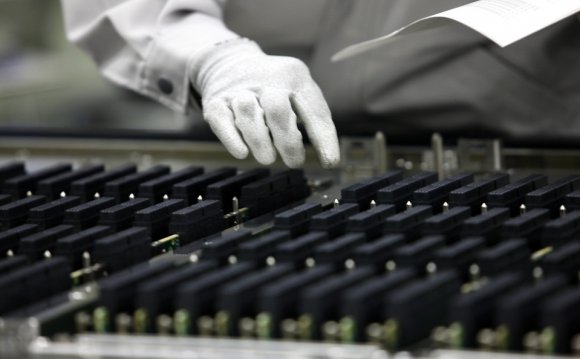
Wafer probing is a process whereby each individual die (chip) on the wafer is tested for defects to identify operable semiconductors for packaging. Packaging, also known as assembly, is the processing of bare semiconductors into finished semiconductors, serving to protect the die and facilitate electrical connections and heat dissipation. We offer a broad range of semiconductor packages meeting the diverse function and cost requirements of our customers.
Final testing of semiconductors ensures that they function properly before being shipped to customers or assembled in electronic products.
Advanced Semiconductor Engineering Inc.(TAIEX: 2311, NYSE: ASX), a leading company of semiconductor assembly and test services.
USI, Inc., a leading electronic manufacturing service provider.
State-of-the-art Process Technologies
As the industry focuses on integrating more functions onto a single chip and chip performance increases with improvements in process technologies, packaging has gained even greater importance. Computing frequency of next generation chips are becoming higher and functions packed onto each chip are increasing. Consequently, requirements for thermal and electrical reliability are rising exponentially. Semiconductor designers need to explore advanced packaging methods to satisfy these requirements.
Innovation and quality are values that ASE prides itself for delivering leading-edge technologies and solutions to customers, meeting their demanding requirements such as electrical performance, heat dissipation, cost and aggressive cycle time. ASE continues to invest the maximum in research and development through its high caliber engineering teams and advanced manufacturing processes.
The advanced manufacturing process technologies that we provide include flip chip and wafer bumping, 300mm wafer bumping and test, Chip Scale Packaging (CSP), 3D packages and System in Package (SiP). We also offer standard products such as PDIP, SOJ, SSOP and PLCC. Our broad product portfolio provides customers the flexibility to select package types that best suit the needs of their chip designs.
ASE has also developed lead-free solutions to eliminate lead in electronic interconnections from both the legislative and competitive sides. We have investigated and tested the performance of various types of lead free solders to generate alternative semiconductor package applications that grant our customers environmentally-friendly chip packages without compromising the reliability.
RELATED VIDEO


Share this Post
latest post
-
 Semiconductor Processing November 26, 2023
 -
 Top Fabless Semiconductor companies October 27, 2023
 -
 Silicon Valley Semiconductor companies September 27, 2023
 -
 New Semiconductor companies August 28, 2023
 -
 List of Semiconductor companies in USA July 29, 2023
 -
 Semiconductor properties June 29, 2023
 -
 Semiconductor industry companies May 30, 2023
 -
 Canadian Semiconductor company April 30, 2023
 -
 Semiconductor companies in Europe March 31, 2023
 -
 Semiconductor jobs in Europe March 1, 2023
 -
 Freescale Semiconductor, Ltd January 30, 2023
 -
 Freescale Semiconductor Patent December 31, 2022
 -
 Freescale Semiconductor news December 1, 2022
 -
 Freescale Semiconductor stock symbol November 1, 2022
 -
 Global Semiconductor company October 28, 2022