 A diode is an electrical device allowing current to move through it in one direction with far greater ease than in the other. The most common kind of diode in modern circuit design is the semiconductor diode, although other diode technologies exist. Semiconductor diodes are symbolized in schematic diagrams such as Figure . The term “diode” is customarily reserved for small signal devices, I ≤ 1 A. The term rectifier is used for power devices, I > 1 A.
Semiconductor diode schematic symbol: Arrows indicate the direction of electron current flow.
When placed in a simple battery-lamp circuit, the diode will either allow or prevent current through the lamp, depending on the polarity of the applied voltage. (Figure )
Diode operation: (a) Current flow is permitted; the diode is forward biased. (b) Current flow is prohibited; the diode is reversed biased.
When the polarity of the battery is such that electrons are allowed to flow through the diode, the diode is said to be forward-biased. Conversely, when the battery is “backward” and the diode blocks current, the diode is said to be reverse-biased. A diode may be thought of as like a switch: “closed” when forward-biased and “open” when reverse-biased.
 Oddly enough, the direction of the diode symbol’s “arrowhead” points against the direction of electron flow. This is because the diode symbol was invented by engineers, who predominantly use conventional flow notation in their schematics, showing current as a flow of charge from the positive (+) side of the voltage source to the negative (-). This convention holds true for all semiconductor symbols possessing “arrowheads:” the arrow points in the permitted direction of conventional flow, and against the permitted direction of electron flow.
Diode behavior is analogous to the behavior of a hydraulic device called a check valve. A check valve allows fluid flow through it in only one direction as in Figure .
Hydraulic check valve analogy: (a) Electron current flow permitted. (b) Current flow prohibited.
Check valves are essentially pressure-operated devices: they open and allow flow if the pressure across them is of the correct “polarity” to open the gate (in the analogy shown, greater fluid pressure on the right than on the left). If the pressure is of the opposite “polarity, ” the pressure difference across the check valve will close and hold the gate so that no flow occurs.
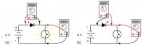
 Like check valves, diodes are essentially “pressure-” operated (voltage-operated) devices. The essential difference between forward-bias and reverse-bias is the polarity of the voltage dropped across the diode. Let’s take a closer look at the simple battery-diode-lamp circuit shown earlier, this time investigating voltage drops across the various components in Figure .
Diode circuit voltage measurements: (a) Forward biased. (b) Reverse biased.
A forward-biased diode conducts current and drops a small voltage across it, leaving most of the battery voltage dropped across the lamp. If the battery’s polarity is reversed, the diode becomes reverse-biased, and drops all of the battery’s voltage leaving none for the lamp. If we consider the diode to be a self-actuating switch (closed in the forward-bias mode and open in the reverse-bias mode), this behavior makes sense. The most substantial difference is that the diode drops a lot more voltage when conducting than the average mechanical switch (0.7 volts versus tens of millivolts).
This forward-bias voltage drop exhibited by the diode is due to the action of the depletion region formed by the P-N junction under the influence of an applied voltage.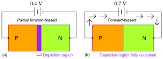 If no voltage applied is across a semiconductor diode, a thin depletion region exists around the region of the P-N junction, preventing current flow. (Figure (a)) The depletion region is almost devoid of available charge carriers, and acts as an insulator:
Diode representations: PN-junction model, schematic symbol, physical part.
The schematic symbol of the diode is shown in Figure (b) such that the anode (pointing end) corresponds to the P-type semiconductor at (a). The cathode bar, non-pointing end, at (b) corresponds to the N-type material at (a). Also note that the cathode stripe on the physical part (c) corresponds to the cathode on the symbol.
If a reverse-biasing voltage is applied across the P-N junction, this depletion region expands, further resisting any current through it. (Figure )
Depletion region expands with reverse bias.
Conversely, if a forward-biasing voltage is applied across the P-N junction, the depletion region collapses becoming thinner. The diode becomes less resistive to current through it. In order for a sustained current to go through the diode; though, the depletion region must be fully collapsed by the applied voltage. This takes a certain minimum voltage to accomplish, called the forward voltage as illustrated in Figure .
RELATED VIDEO

Share this Post
latest post
-
 Semiconductor Processing November 26, 2023
 -
 Top Fabless Semiconductor companies October 27, 2023
 -
 Silicon Valley Semiconductor companies September 27, 2023
 -
 New Semiconductor companies August 28, 2023
 -
 List of Semiconductor companies in USA July 29, 2023
 -
 Semiconductor properties June 29, 2023
 -
 Semiconductor industry companies May 30, 2023
 -
 Canadian Semiconductor company April 30, 2023
 -
 Semiconductor companies in Europe March 31, 2023
 -
 Semiconductor jobs in Europe March 1, 2023
 -
 Freescale Semiconductor, Ltd January 30, 2023
 -
 Freescale Semiconductor Patent December 31, 2022
 -
 Freescale Semiconductor news December 1, 2022
 -
 Freescale Semiconductor stock symbol November 1, 2022
 -
 Global Semiconductor company October 28, 2022