
The PN Junction Diode
The effect described in the previous tutorial is achieved without any external voltage being applied to the actual PN junction resulting in the junction being in a state of equilibrium. However, if we were to make electrical connections at the ends of both the N-type and the P-type materials and then connect them to a battery source, an additional energy source now exists to overcome the potential barrier.
The effect of adding this additional energy source results in the free electrons being able to cross the depletion region from one side to the other. The behaviour of the PN junction with regards to the potential barrier’s width produces an asymmetrical conducting two terminal device, better known as the PN Junction Diode.
A PN Junction Diode is one of the simplest Semiconductor Devices around, and which has the characteristic of passing current in only one direction only. However, unlike a resistor, a diode does not behave linearly with respect to the applied voltage as the diode has an exponential current-voltage ( I-V ) relationship and therefore we can not described its operation by simply using an equation such as Ohm’s law.
 If a suitable positive voltage (forward bias) is applied between the two ends of the PN junction, it can supply free electrons and holes with the extra energy they require to cross the junction as the width of the depletion layer around the PN junction is decreased.
By applying a negative voltage (reverse bias) results in the free charges being pulled away from the junction resulting in the depletion layer width being increased. This has the effect of increasing or decreasing the effective resistance of the junction itself allowing or blocking current flow through the diode.
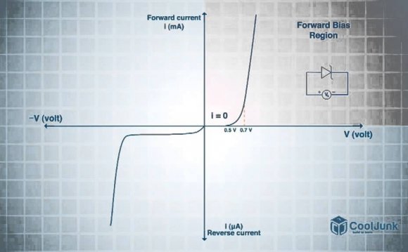
Then the depletion layer widens with an increase in the application of a reverse voltage and narrows with an increase in the application of a forward voltage. This is due to the differences in the electrical properties on the two sides of the PN junction resulting in physical changes taking place. One of the results produces rectification as seen in the PN junction diodes static I-V (current-voltage) characteristics. Rectification is shown by an asymmetrical current flow when the polarity of bias voltage is altered as shown below.
Junction Diode Symbol and Static I-V Characteristics.
But before we can use the PN junction as a practical device or as a rectifying device we need to firstly bias the junction, ie connect a voltage potential across it. On the voltage axis above, “Reverse Bias” refers to an external voltage potential which increases the potential barrier. An external voltage which decreases the potential barrier is said to act in the “Forward Bias” direction.


RELATED VIDEO

Share this Post
latest post
-
 Semiconductor Processing November 26, 2023
 -
 Top Fabless Semiconductor companies October 27, 2023
 -
 Silicon Valley Semiconductor companies September 27, 2023
 -
 New Semiconductor companies August 28, 2023
 -
 List of Semiconductor companies in USA July 29, 2023
 -
 Semiconductor properties June 29, 2023
 -
 Semiconductor industry companies May 30, 2023
 -
 Canadian Semiconductor company April 30, 2023
 -
 Semiconductor companies in Europe March 31, 2023
 -
 Semiconductor jobs in Europe March 1, 2023
 -
 Freescale Semiconductor, Ltd January 30, 2023
 -
 Freescale Semiconductor Patent December 31, 2022
 -
 Freescale Semiconductor news December 1, 2022
 -
 Freescale Semiconductor stock symbol November 1, 2022
 -
 Global Semiconductor company October 28, 2022