
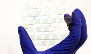
 "The electrical performance of our materials was comparable to that of reported results from single crystals of molybdenum disulfide, but instead of a tiny crystal, here we have a 4-inch wafer, " says Jiwoong Park. Above: A molybdenum disulphide device array on a transparent silica wafer. (Credit: Kibum Kang/Cornell)
Making thin films out of semiconducting materials is analogous to how ice grows on a windowpane: when the conditions are just right, the semiconductor grows in flat crystals that slowly fuse together, eventually forming a continuous film.
This process of film deposition is common for traditional semiconductors like silicon or gallium arsenide—the basis of modern electronics.
Now, scientists pushing the limits for how thin they can go have demonstrated a way to create a new kind of semiconductor thin film that retains its electrical properties even when it is just atoms thick.
Ultrathin sheets
“The electrical performance of our materials was comparable to that of reported results from single crystals of molybdenum disulfide, but instead of a tiny crystal, here we have a 4-inch wafer, ” says Jiwoong Park, associate professor of chemistry and chemical biology at Cornell University.
Molybdenum disulfide, which is garnering worldwide interest for its excellent electrical properties, has previously been grown only in disjointed, “archipelago”-like single crystal formations. But making smooth, flat, ultrathin sheets, like paper, is the ultimate goal, and the bridge to actual devices, Park says.
As reported online in the journal, the researchers pulled off the feat by tuning the growth conditions of their films using a technique called metal organic chemical vapor deposition (MOCVD). Already used widely in industry, but with different materials, it starts with a powdery precursor, forms a gas, and sprinkles single atoms onto a substrate, one layer at a time.
‘Kitchen’ experiments
The researchers systematically optimized the technique to make the films, tweaking conditions and temperatures not unlike experimenting in the kitchen. The crystals grew perfectly stitched together, but only with a little bit of hydrogen and in completely dry conditions, for example.
In addition to advanced optical imaging techniques, researchers led by coauthor David Muller, professor of applied and engineering physics, contributed advanced transmission electron microscopy to test and characterize the quality of the films as they went along.
RELATED VIDEO


RELATED FACTS
-
 Engineers in Prof. Krishna Saraswat’s laboratory have developed a novel method for forming semiconductor thin films at low temperature (
- Engineers in Prof. Krishna Saraswat’s laboratory have developed a novel method for forming semiconductor thin films at low temperature (
- This invention provides a method of forming semiconductor films on dielectrics at temperatures below 400.degree.
Share this Post
latest post
-
 Semiconductor Processing November 26, 2023
 -
 Top Fabless Semiconductor companies October 27, 2023
 -
 Silicon Valley Semiconductor companies September 27, 2023
 -
 New Semiconductor companies August 28, 2023
 -
 List of Semiconductor companies in USA July 29, 2023
 -
 Semiconductor properties June 29, 2023
 -
 Semiconductor industry companies May 30, 2023
 -
 Canadian Semiconductor company April 30, 2023
 -
 Semiconductor companies in Europe March 31, 2023
 -
 Semiconductor jobs in Europe March 1, 2023
 -
 Freescale Semiconductor, Ltd January 30, 2023
 -
 Freescale Semiconductor Patent December 31, 2022
 -
 Freescale Semiconductor news December 1, 2022
 -
 Freescale Semiconductor stock symbol November 1, 2022
 -
 Global Semiconductor company October 28, 2022