 I must confess that until recently, I wasn’t well-versed in semiconductor physics or technology. While it’s rather easy to understand what a transistor does and some of the terminology thrown around, going deeper was tough. A great deal of the information on the internet is simply too cryptic to understand, even for those that want to learn. Seeing as how this site is all about the results of semiconductor physics and technology, this was the best place to share the knowledge that I've acquired.
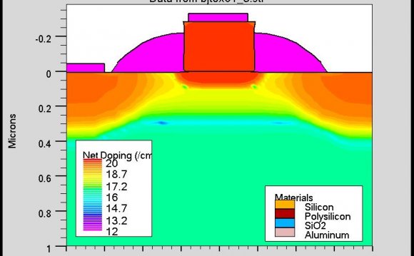
The simplest place to start is the materials. Silicon is incredibly important as a material in the industry because it’s a semiconductor. Of course, the name is self-explanatory, but there’s more to it. The key here is the band structure. Band structure refers to the “bands” of energy levels that form due to the sheer number of orbital states that can be occupied in molecules. Those that understand how electron orbitals work will point out that each energy level is discrete, but due to the sheer number of orbital configurations, a seemingly continuous distribution of energy can be seen. However, relatively large gaps still exist; known as a band gap, these are an energy state that an electron cannot occupy.
The question now is why this matters. The reason why it does matter is because of the Fermi level, or EF in the photo above. The Fermi level refers to the total chemical potential energy for a system of electrons at absolute zero. If the band lies above the Fermi level, electrons in the band can be delocalized from the atom, which means that it can carry current. This band is called a conduction band. If the band is below the Fermi level, this means that the electron is bound to an atom. This band would be a valence band.
 Intrinsically, a semiconductor should have its Fermi level at the midpoint of the band gap. This is true of both insulators and intrinsic semiconductors, but a semiconductor’s band gap is extremely small. In fact, it’s small enough that electrons can jump the band gap as seen in the photo above because of thermal energy that will always exist in real world situations. While this property alone isn't particularly useful for digital logic, doping a semiconductor can have significant effects on the band structure. This means that the distribution of electrons in the valence band or conduction band will change.
This is where I have to introduce even more terminology. Depending on how the distribution is changed, a semiconductor is dubbed either a p-type or n-type semiconductor. If the band structure is such that free electrons are more easily generated, it becomes an n-type semiconductor. If the structure is such that electron “holes” are generated, it becomes a p-type semiconductor.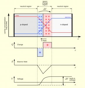 In this case, electron holes refers to a place where an electron could exist, but doesn’t. Such a hole still conducts current. Look carefully at the p-type diagram once again. Because the valence band is so close to the Fermi level, electrons tend to stay in the valence band at lower orbitals. This is means that there are "holes" where an electron could be, which makes it a charge carrier. It's also worth noting that the diagram above isn't totally accurate, as doping normally introduces more bands instead of shifting their positions, but the concept is the same.
What really makes things interesting is when a p-type and n-type semiconductor are placed next to each other. Because p-type semiconductors tend to have electron holes and n-type semiconductors tend to have an excess of electrons, there will be a diffusion of holes and electrons to try and equalize charge at the junction. Because of this diffusion process, the area around the junction becomes charged positively at the n-doped region and negatively at the p-doped region. This happens because the n-doped region is losing electrons, making the area positive while the p-doped region is losing holes, therefore becoming negative. The result is that an electric field is generated which opposes this diffusion and eventually reaches equilibrium. The area where this process occurs is called the depletion layer, as these ionized areas are stripped of charge carriers and therefore unable to carry current with the band structure that already exists.
This p-n junction is incredibly important in solid state electronics. In fact, the system we just described can be used as a diode, which is a device that only allows current to flow in a single direction. If a battery is connected with the positive terminal at the p-type semiconductor and the negative on the n-type semiconductor, the holes in the p-type and the electrons in n-type are all pushed towards the junction, which causes the depletion zone to shrink. This means that the electric field repelling the current decreases, and current is allowed to flow across the junction.
RELATED VIDEO

![[PDF] The Physics of Semiconductors: An Introduction](/img/video/pdf_the_physics_of_semiconductors_an.jpg)

Share this Post
latest post
-
 Semiconductor Processing November 26, 2023
 -
 Top Fabless Semiconductor companies October 27, 2023
 -
 Silicon Valley Semiconductor companies September 27, 2023
 -
 New Semiconductor companies August 28, 2023
 -
 List of Semiconductor companies in USA July 29, 2023
 -
 Semiconductor properties June 29, 2023
 -
 Semiconductor industry companies May 30, 2023
 -
 Canadian Semiconductor company April 30, 2023
 -
 Semiconductor companies in Europe March 31, 2023
 -
 Semiconductor jobs in Europe March 1, 2023
 -
 Freescale Semiconductor, Ltd January 30, 2023
 -
 Freescale Semiconductor Patent December 31, 2022
 -
 Freescale Semiconductor news December 1, 2022
 -
 Freescale Semiconductor stock symbol November 1, 2022
 -
 Global Semiconductor company October 28, 2022