Suppose, in any pure or intrinsic germanium or silicon semiconductor any pentavalent impurity is added. The pentavalent impurities are those which have atoms with five (5) balance electrons. As soon as the impurity is added to the semiconductor, the impurity atoms will replace some of the semiconductor atoms in crystal structure. Now four (4) of the five (5) valance electrons of impurity atom will involve in bonding with four neighborhood semiconductor atoms but the fifth one electron will not find any place to occupy. This fifth electron of the impurity atom can be made available as free electron or negative charge carrier even if very small amount of energy is applied. The energy required to detach the this fifth electron from its parent atom is in the range of 0.01 eV (electron volt) to 0.05 eV (electron volt). Antimony, phosphorus and arsenic are normally and commercially used pentavalent impurities for semiconductor. As pentavalent impurities contribute or donate electrons to the semiconductor these are called donor impurities and similarly as these impurities contribute negative charge carriers in the semiconductor this is also referred as n - type impurities. The semiconductor doped with n - type impurities is called n - type semiconductor.
N - Type Semiconductor
When n type or donor impurities are added to the semiconductor, the width of the forbidden energy gap in the lattice structure is reduced. Due to addition of donor atoms, allowable energy levels are introduced a very small distance below the conduction band as is shown in the figure below. This new allowable levels are discrete because the added impurity atoms are placed far apart and hence there interaction is small. In the germanium the discrete allowable energy level or forbidden energy gap is only 0.01 eV (electron volt) and that for silicon is 0.05 eV (electron volt) at room temperature. So it is predictable that at room temperature the fifth electron of all donor atoms are in conduction band. On the other hand the increased number of negative charge carriers i.e. electrons in the semiconductor causes decrease in number of holes. Number of holes per unit volume in an n - type semiconductor is even lower than that in the same unit volume of intrinsic semiconductor at same temperature. This is because of excess electrons, there will be higher rate of recombination of electron-hole pairs than that in pure or intrinsic semiconductor.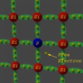
P - Type Semiconductor
If instead of pentavalent impurity, trivalent impurity is added to the intrinsic semiconductor, then instead of excess electrons there will be excess holes created in the crystal. This is because when a trivalent impurity is added to the semiconductor crystal, the trivalent atoms will replace some of the tetravalent semiconductor atoms. The three (3) valance electrons of trivalent impurity atom will make bond with three neighborhood semiconductor atoms. Hence there will be lack of electron in one bond of the fourth neighboring semiconductor atom which contributes a whole to the crystal. Since trivalent impurities contribute excess holes to semiconductor crystal, and these holes can accept electrons, these impurities are referred as acceptor impurities. As the holes virtually carry positive charge, the said impurities are referred as positive - type or p - type impurities and the semiconductor with p - type impurities is called p - type semiconductor. When trivalent impurities are added to a semiconductor, a discrete energy level is created just above the valance band of the semiconductor. As the gap between valance energy level and the new discrete energy level created by impurity is quite less, electron can easily migrate to the new higher energy level with help of very small amount of external energy. When an electron is migrated to new energy level, it creates a vacancy in the valance band behind it and this contributes hold to the semiconductor.It is to be noted that when an n type impurity is added to semiconductor, there will be excess electron is a crystal but it does not mean that there would not be any hole. Due to intrinsic nature of semiconductor at room temperature there are always be some electron-holes pairs in the semiconductor. Due to addition of n - type impurities, the electrons will be added to that electron hole pairs and also the number of holes reduced excess recombination for excess electrons. And hence the total number of negative charge carriers or free electrons will be more than that of holes in n type semiconductor. That is why in n - type semiconductor electrons are called majority charge carriers whereas poles are called minority charge carriers. Similarly in p - type semiconductor, holes are called the majority charge carriers and electrons are called minority charge carriers.
RELATED VIDEO

Share this Post
latest post
-
 Semiconductor Processing November 26, 2023
 -
 Top Fabless Semiconductor companies October 27, 2023
 -
 Silicon Valley Semiconductor companies September 27, 2023
 -
 New Semiconductor companies August 28, 2023
 -
 List of Semiconductor companies in USA July 29, 2023
 -
 Semiconductor properties June 29, 2023
 -
 Semiconductor industry companies May 30, 2023
 -
 Canadian Semiconductor company April 30, 2023
 -
 Semiconductor companies in Europe March 31, 2023
 -
 Semiconductor jobs in Europe March 1, 2023
 -
 Freescale Semiconductor, Ltd January 30, 2023
 -
 Freescale Semiconductor Patent December 31, 2022
 -
 Freescale Semiconductor news December 1, 2022
 -
 Freescale Semiconductor stock symbol November 1, 2022
 -
 Global Semiconductor company October 28, 2022