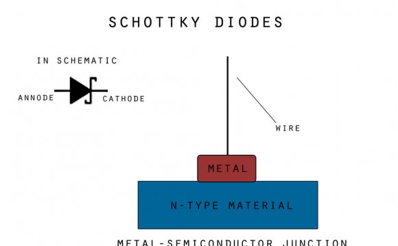
A Schottky barrier, named after Walter H. Schottky, is a potential energy barrier for electrons formed at a metal–semiconductor junction. Schottky barriers have rectifying characteristics, suitable for use as a diode. One of the primary characteristics of a Schottky barrier is the Schottky barrier height, denoted by ΦB (see figure). The value of ΦB depends on the combination of metal and semiconductor.
Not all metal–semiconductor junctions form a rectifying Schottky barrier; a metal–semiconductor junction that conducts current in both directions without rectification, perhaps due to its Schottky barrier being too low, is called an ohmic contact.
Physics of formation[edit]
The barrier between a metal and a semiconductor is naively predicted by the Schottky-Mott rule to be proportional to the difference of the metal-vacuum work function and the semiconductor-vacuum electron affinity. In practice, however, most metal-semiconductor interfaces do not follow this rule to the predicted degree. Instead, the chemical termination of the semiconductor crystal against a metal creates electron states within its band gap. The nature of these metal-induced gap states and their occupation by electrons tends to pin the center of the band gap to the Fermi level, an effect known as Fermi level pinning. Thus the heights of the Schottky barriers in metal-semiconductor contacts often show little dependence on the value of the semiconductor or metal work functions, in strong contrast to the Schottky-Mott rule. Different semiconductors exhibit this Fermi level pinning to the different degrees, but a technological consequence is that ohmic contacts are usually difficult to form in important semiconductors such as silicon and gallium arsenide. Non-ohmic contacts present a parasitic resistance to current flow that consumes energy and lowers device performance.
Rectifying properties[edit]
In a rectifying Schottky barrier, the barrier is high enough that there is a depletion region in the semiconductor, near the interface. This gives the barrier a high resistance when small voltage biases are applied to it. Under large voltage bias, the electric current flowing through the barrier is essentially governed by the laws of thermionic emission, combined with the fact that the Schottky barrier is fixed relative to the metal's Fermi level.
Forward bias: thermally excited electrons are able to spill into the metal.
Reverse bias: electrons are blocked from entering the semiconductor.
- Under forward bias, there are many thermally excited electrons in the semiconductor that are able to pass over the barrier. The passage of these electrons over the barrier (without any electrons coming back) corresponds to a current in the opposite direction. The current rises very rapidly with bias, however at high biases the series resistance of the semiconductor can start to limit the current.
- Under reverse bias, there is a small leakage current as some thermally excited electrons in the metal have enough energy to surmount the barrier. To first approximation this current should be constant (as in the Shockley diode equation); however, current rises gradually with reverse bias due to a weak barrier lowering (similar to the vacuum Schottky effect). At very high biases, the depletion region breaks down.
Note: the discussion above is for a Schottky barrier to an n-type semiconductor; similar considerations apply for a p-type semiconductor.
The current-voltage relationship is qualitatively the same as with a p-n junction, however the physical process is somewhat different.
For a very high Schottky barrier (in this case, almost as high as the band gap), the forward bias current is carried by minority carrier injection (the white arrow shows the injection of an electron hole into the semiconductor's valence band).Minority carrier injection[edit]
For very high Schottky barriers where ΦB is a significant fraction of the band gap of the semiconductor, the forward bias current may instead be carried "underneath" the Schottky barrier, as minority carriers in the semiconductor.
Devices[edit]
A Schottky diode is a single metal–semiconductor junction, used for its rectifying properties. Schottky diodes are often the most suitable kind of diode when a low forward voltage drop is desired, such as in a high efficiency DC power supply. Also, because of their majority-carrier conduction mechanism, Schottky diodes can achieve greater switching speeds than p–n junction diodes, making them appropriate to rectify high-frequency signals.
A bipolar junction transistor with a Schottky barrier between the base and the collector is known as a Schottky transistor. Because the junction voltage of the Schottky barrier is small, the transistor is prevented from saturating too deeply, which improves the speed when used as a switch. This is the basis for the Schottky and Advanced Schottky TTL families, as well as their low power variants.
A MESFET or metal–semiconductor FET uses a reverse-biased Schottky barrier to provide a depletion region that pinches off a conducting channel buried inside the semiconductor (similar to the JFET where instead a p–n junction provides the depletion region). A variant of this device is the high-electron-mobility transistor (HEMT), which also utilizes a heterojunction to provide a device with extremely high conductance.
A Schottky barrier carbon nanotube FET uses the non-ideal contact between a metal and a carbon nanotube to form a Schottky barrier that can be used to make extremely small Schottky diodes, transistors, and similar electronic devices with unique mechanical and electronic properties.
Schottky barriers can also be used to characterize a semiconductor. In the depletion region of the Schottky barrier, dopants remain ionized and give rise to a "space charge" which in turn give rise to a capacitance of the junction. The metal–semiconductor interface and the opposite boundary of the depleted area act like two capacitor plates, with the depletion region acting as a dielectric. By applying a voltage to the junction it is possible to vary the depletion width and vary the capacitance, used in capacitance voltage profiling. By analyzing the speed at which the capacitance responds to changes in voltage, it is possible to obtain information about dopants and other defects, a technique known as deep-level transient spectroscopy.
RELATED VIDEO


Share this Post
latest post
-
 Semiconductor Processing November 26, 2023
 -
 Top Fabless Semiconductor companies October 27, 2023
 -
 Silicon Valley Semiconductor companies September 27, 2023
 -
 New Semiconductor companies August 28, 2023
 -
 List of Semiconductor companies in USA July 29, 2023
 -
 Semiconductor properties June 29, 2023
 -
 Semiconductor industry companies May 30, 2023
 -
 Canadian Semiconductor company April 30, 2023
 -
 Semiconductor companies in Europe March 31, 2023
 -
 Semiconductor jobs in Europe March 1, 2023
 -
 Freescale Semiconductor, Ltd January 30, 2023
 -
 Freescale Semiconductor Patent December 31, 2022
 -
 Freescale Semiconductor news December 1, 2022
 -
 Freescale Semiconductor stock symbol November 1, 2022
 -
 Global Semiconductor company October 28, 2022