 Interconnect requirements for the 22nm technology node and beyond, driven by shrinking FEOL geometry, push the limits of unit process tools for BEOL as well as FEOL. BEOL tools for WLCSP (Wafer level chip scale packaging) take advantage of many lithographic techniques utilized in the manufacture of the chip in the Front End of Line (FEOL).
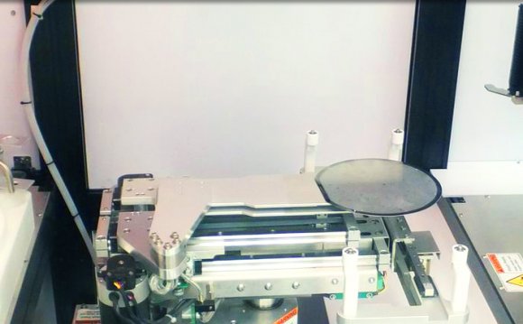
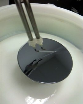
One of the principal processes utilized in the back end of line is the Photolithographic process to perform such steps as redistribution layer, under bump metallization, and bump formation. An example of bump formation during the lift-off resist process is shown below:
Semiconductor photolithographic processing steps are discussed below.
Wafer Handling steps
- The substrate is automatically withdrawn from a cassette which may be in a SMIF pod.
 Alternatively for 300mm wafers a FOUP opener may be employed.
 - The substrate is precisely positioned on a rotatable vacuum chuck such that the center of the substrate is coincident with the center of rotation of the vacuum chuck.
- After photoresist is applied the substrate is baked (normally on a heated plate provided for the purpose.)
- The substrate is returned to the cassette or to a second cassette.
Source: www.s-cubed.com
Share this Post
latest post
-
 Semiconductor Processing November 26, 2023
 -
 Top Fabless Semiconductor companies October 27, 2023
 -
 Silicon Valley Semiconductor companies September 27, 2023
 -
 New Semiconductor companies August 28, 2023
 -
 List of Semiconductor companies in USA July 29, 2023
 -
 Semiconductor properties June 29, 2023
 -
 Semiconductor industry companies May 30, 2023
 -
 Canadian Semiconductor company April 30, 2023
 -
 Semiconductor companies in Europe March 31, 2023
 -
 Semiconductor jobs in Europe March 1, 2023
 -
 Freescale Semiconductor, Ltd January 30, 2023
 -
 Freescale Semiconductor Patent December 31, 2022
 -
 Freescale Semiconductor news December 1, 2022
 -
 Freescale Semiconductor stock symbol November 1, 2022
 -
 Global Semiconductor company October 28, 2022