In the of the series, we discussed electrical die sorting (EDS), one of the last stages of semiconductor fabrication. Today, we will cover the packaging and package testing processes as we wrap up our series and ship off our completed semiconductor.
Plugs with Pins and Protection from Dings
Semiconductor packaging involves enclosing integrated circuits (IC) in a form factor that can fit into a specific device. Since a semiconductor chip, or IC, is mounted on a circuit board or used in an electronic device, it needs to go through an electrical packaging process to be molded into the appropriate design and form.
If the IC were the human brain, its packaging would be the nervous system and skeletal structure.
In other words, semiconductor packaging serves a variety of purposes: ensuring the inter-terminal connection, supplying electricity, and providing heat resistance and protection for the IC. The packaging also ensures protection from external factors, including humidity, chemicals, impact and vibration.
Now, let’s take a look at how the packaging process works.
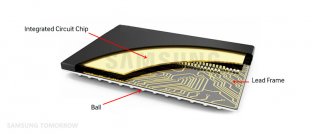
First, wafers are cut into individual chips with a diamond cutter. Faulty chips marked during the inking process are left behind while functional chips are placed on a lead frame or PCB (Printed Circuit Board), which are then attached with balls that provide an electrical connection.
The lead frame delivers electrical signals between the semiconductor chip and the board while offering structural support to protect the chip from external humidity or impact. Chips are connected to the lead frame with fine gold wires in a process called wire bonding.
After the chips are attached to the lead frames, they undergo the molding process, which gives them their exterior shells. At this stage, intense heat is applied to an epoxy molding compound (EMC) made of resin, which is liquefied and shaped into the desired form.
At last, the semiconductor chips resemble the ones we see inside our electronic devices.
The Last Stretch: Package Testing
Once the packaging process is complete, we have to determine if the package works properly. So, it’s time to move on to the last stage, the package test, in which our packaged semiconductor goes through the final quality assurance procedures.
The semiconductor chips are put in a device where they are tested under various conditions of voltage, electrical signals and temperature. In doing so, we can measure their electrical and functional characteristics as well as their performance to detect any defects.
We also collect and analyze the data accumulated during the test and give feedback to the teams overseeing the manufacturing and assembly processes to further improve the quality of our products.
RELATED VIDEO


Share this Post
latest post
-
 Semiconductor Processing November 26, 2023
 -
 Top Fabless Semiconductor companies October 27, 2023
 -
 Silicon Valley Semiconductor companies September 27, 2023
 -
 New Semiconductor companies August 28, 2023
 -
 List of Semiconductor companies in USA July 29, 2023
 -
 Semiconductor properties June 29, 2023
 -
 Semiconductor industry companies May 30, 2023
 -
 Canadian Semiconductor company April 30, 2023
 -
 Semiconductor companies in Europe March 31, 2023
 -
 Semiconductor jobs in Europe March 1, 2023
 -
 Freescale Semiconductor, Ltd January 30, 2023
 -
 Freescale Semiconductor Patent December 31, 2022
 -
 Freescale Semiconductor news December 1, 2022
 -
 Freescale Semiconductor stock symbol November 1, 2022
 -
 Global Semiconductor company October 28, 2022